|
|
|
PDF NDS8961 Data sheet ( Hoja de datos )
| Número de pieza | NDS8961 | |
| Descripción | Dual N-Channel Enhancement Mode Field Effect Transistor | |
| Fabricantes | Fairchild | |
| Logotipo | ||
Hay una vista previa y un enlace de descarga de NDS8961 (archivo pdf) en la parte inferior de esta página. Total 10 Páginas | ||
|
No Preview Available !
June 1997
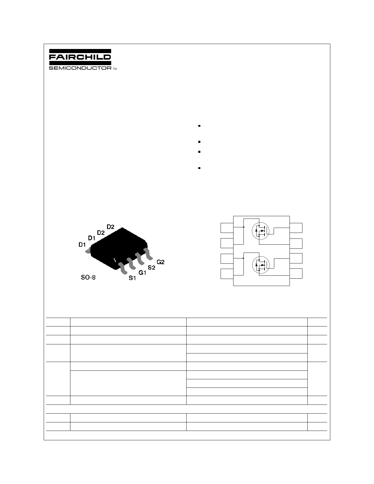
NDS8961
Dual N-Channel Enhancement Mode Field Effect Transistor
General Description
SO-8 N-Channel enhancement mode power field effect
transistors are produced using Fairchild's proprietary, high cell
density, DMOS technology. This very high density process is
especially tailored to minimize on-state resistance and provide
superior switching performance.These devices are particularly
suited for low voltage applications such as DC motor control
and DC/DC conversion where fast switching, low in-line power
loss, and resistance to transients are needed.
Features
3.1 A, 30 V. RDS(ON) = 0.1 Ω @ VGS = 10 V
RDS(ON) = 0.15 Ω @ VGS = 4.5 V.
High density cell design for extremely low RDS(ON).
High power and current handling capability in a widely used
surface mount package.
Dual MOSFET in surface mount package.
____________________________________________________________________________________________
54
63
72
81
Absolute Maximum Ratings TA = 25°C unless otherwise noted
Symbol Parameter
VDSS Drain-Source Voltage
VGSS Gate-Source Voltage
ID Drain Current - Continuous
- Pulsed
(Note 1a)
PD Power Dissipation for Dual Operation
Power Dissipation for Single Operation
(Note 1a)
(Note 1b)
(Note 1c)
TJ,TSTG
Operating and Storage Temperature Range
THERMAL CHARACTERISTICS
RθJA Thermal Resistance, Junction-to-Ambient (Note 1a)
RθJC Thermal Resistance, Junction-to-Case (Note 1)
© 1997 Fairchild Semiconductor Corporation
NDS8961
30
±20
3.1
10
2
1.6
1
0.9
-55 to 150
78
40
Units
V
V
A
W
°C
°C/W
°C/W
NDS8961 Rev.D
1 page 
Typical Electrical Characteristics
1.12
1.08
ID = 250µA
1.04
1
0.96
0.92
-50 -25 0 25 50 75 100 125 150
T , JUNCTION TEMPERATURE (°C)
J
Figure 7. Breakdown Voltage Variation with
Temperature.
10
5
VGS =0V
1
0 .1
0 .0 1
0 .0 0 1
TJ = 125°C
25°C
-55°C
0 .0 0 0 1
0
0 .2 0 .4 0.6 0 .8
1
VSD , BODY DIODE FORWARD VOLTAGE (V)
1 .2
Figure 8. Body Diode Forward Voltage Variation
with Current and Temperature.
600
400
2 0 0 Ciss
100
70
50
f = 1 MHz
30 VGS = 0V
Coss
Crss
20
0 .1
0 .2
0 .5 1
2
5 10
V , DRAIN TO SOURCE VOLTAGE (V)
DS
20 30
Figure 9. Capacitance Characteristics.
VIN
VGS
RGEN
G
VDD
RL
D
VOUT
DUT
S
Figure 11. Switching Test Circuit.
10
I D = 3.1A
8
VDS = 5V
10V
15V
6
4
2
0
0246
Q g , GATE CHARGE (nC)
Figure 10. Gate Charge Characteristics.
8
t d(on)
t on
tr
90%
td(off)
toff
tf
90%
VO U T
VIN
10%
10%
50%
10%
90%
INVERTED
50%
PULSE WIDTH
Figure 12. Switching Waveforms.
NDS8961 Rev.D
5 Page | ||
| Páginas | Total 10 Páginas | |
| PDF Descargar | [ Datasheet NDS8961.PDF ] | |
Hoja de datos destacado
| Número de pieza | Descripción | Fabricantes |
| NDS8961 | Dual N-Channel Enhancement Mode Field Effect Transistor | Fairchild |
| Número de pieza | Descripción | Fabricantes |
| SLA6805M | High Voltage 3 phase Motor Driver IC. |
Sanken |
| SDC1742 | 12- and 14-Bit Hybrid Synchro / Resolver-to-Digital Converters. |
Analog Devices |
|
DataSheet.es es una pagina web que funciona como un repositorio de manuales o hoja de datos de muchos de los productos más populares, |
| DataSheet.es | 2020 | Privacy Policy | Contacto | Buscar |