|
|
PDF NCP1560 Data sheet ( Hoja de datos )
| Número de pieza | NCP1560 | |
| Descripción | Full Featured Voltage Mode PWM Controller | |
| Fabricantes | ON | |
| Logotipo |  |
|
Hay una vista previa y un enlace de descarga de NCP1560 (archivo pdf) en la parte inferior de esta página. Total 18 Páginas | ||
|
No Preview Available !
NCP1560
Full Featured Voltage Mode
PWM Controller
The NCP1560 PWM controller contains all the features and
flexibility needed to implement voltage- mode control in high
performance single ended DC/DC converters. This device cost
effectively reduces system part count with the inclusion of a high
voltage start-up regulator that operates over a wide input range of
21.5 V to 150 V. The NCP1560 provides two control outputs, OUT1
which controls the main PWM switch and OUT2 with adjustable
over-lap delay, which can control a synchronous rectifier switch or an
active clamp/reset switch. Other distinctive features include: two
mode over current protection, line under/over voltage lockout, fast
line feedforward, soft start and a maximum duty cycle limit.
Features
• Minimum Operating Voltage of 21.5 V
• Internal High Voltage Start-up Regulator
• Dual Control Outputs with Adjustable Overlap Delay
• Single Resistor Oscillator Frequency Setting
• Fast Line Feedforward
• Line Under/Over Voltage Lockout
• Dual Mode Over Current Protection
• Programmable Maximum Duty Cycle Control
• Maximum Duty Cycle Proportional to Line Voltage
• Programmable Soft Start
• Precision 5.0 V Reference
Typical Applications
• Telecommunication Power Converters
• Industrial Power Converters
• High Voltage Power Modules
• +42 V Automotive Systems
• Control Driven Synchronous Rectifier Power Converters
http://onsemi.com
16
1
MARKING
DIAGRAM
16
SO-16
D SUFFIX
CASE 751B
NCP1560
AWLYWW
1
NCP1560 = Device Code
A = Assembly Location
WL = Wafer Lot
Y = Year
WW = Work Week
ORDERING INFORMATION
Device
Package
Shipping
NCP1560HDR2 SO-16 2500/Tape & Reel
© Semiconductor Components Industries, LLC, 2003
January, 2003 - Rev. 5
1
Publication Order Number
NCP1560/D
1 page 
NCP1560
MAXIMUM RATINGS (Note 1)
Rating
Symbol
Value
Unit
Input Line Voltage
Auxiliary Supply Voltage
Auxiliary Supply Input Current
OUT1 and OUT2 Voltage
OUT1 and OUT2 Output Current
5.0 V Reference Voltage
5.0 V Reference Output Current
All Other Inputs/Outputs Voltage
All Other Inputs/Outputs Current
Operating Junction Temperature
Storage Temperature Range
Power Dissipation at TA = 25°C
Thermal Resistance, Junction to Ambient
Vin
VAUX
IAUX
VOUT
IOUT
VREF
IREF
VIO
IIO
TJ
Tstg
PD
RqJA
-0.3 to 150
-0.3 to 16
35
-0.3 to (VAUX + 0.3 V)
10
-0.3 to 6.0
6.0
-0.3 to VREF
10
-40 to 125
-55 to 150
0.77
130
V
V
mA
V
mA
V
mA
V
mA
°C
°C
W
°C/W
1. Maximum Ratings are those values beyond which damage to the device may occur. Exposure to these conditions or conditions beyond those
indicated may adversely affect device reliability. Functional operation under absolute maximum-rated conditions is not implied. Functional
operation should be restricted to the Recommended Operating Conditions.
A. This device series contains ESD protection and exceeds the following tests:
Pin 1 is the HV start-up of the device and is rated to the max rating of the part, or 150 V.
Machine Model Method 150 V.
Pins 2-16: Human Body Model 4000 V per MIL-STD-883, Method 3015.
Machine Model Method 200 V.
http://onsemi.com
5
5 Page 
NCP1560
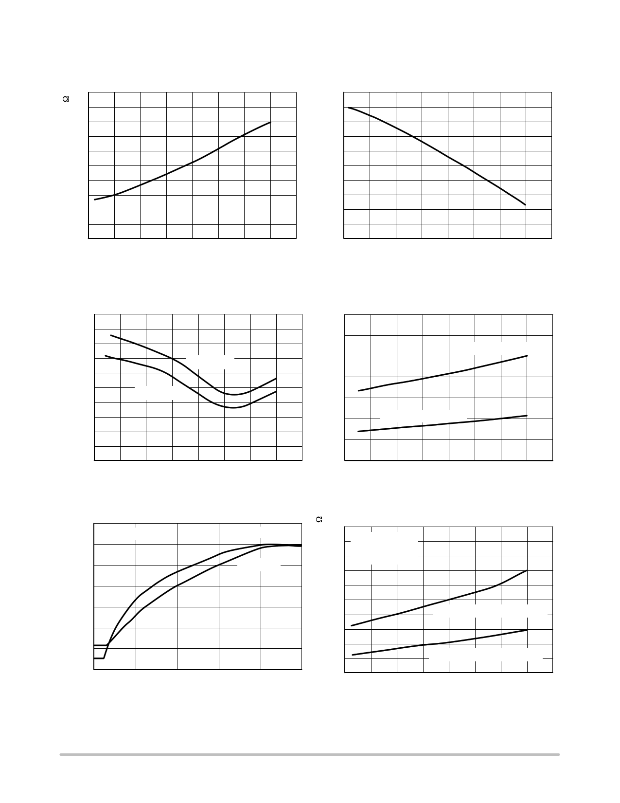
Typical Characteristics
50 0.85
40 0.75
30 0.65
20 0.55
10 0.45
0
-50 -25 0 25 50 75 100 125 150
TJ, JUNCTION TEMPERATURE (°C)
Figure 21. VEA Input Resistance versus
Junction Temperature
0.35
-50
-25 0 25 50 75 100 125 150
TJ, JUNCTION TEMPERATURE (°C)
Figure 22. PWM Comparator Lower Input
Threshold versus Junction Temperature
5.03
5.01
4.99
4.97
IREF = 0 mA
IREF = 6 mA
4.95
4.93
-50 -25
0 25 50 75 100 125 150
TJ, JUNCTION TEMPERATURE (°C)
Figure 23. Reference Voltage versus Junction
Temperature
225
TJ = 25°C
200
LEADING
175 TRAILING
150
125
100
75
50
0 200 400 600 800 1000
RD, DELAY RESISTOR (kW)
Figure 25. Outputs Overlap Delay versus
Delay Resistor
350
300
RD = 1 MW, LEADING
250
200
150
100 RD = 60 kW, LEADING
50
0
-50 -25
0 25 50 75 100 125 150
TJ, JUNCTION TEMPERATURE (°C)
Figure 24. Outputs Overlap Delay versus
Junction Temperature
200
Vin = 36 V
VAUX = 12 V
160 RMDP = 100 kW
120
80 RSRC (VEA = 0 V, VOUT = 10 V)
40
RSNK (VEA = 3 V, VOUT = 2 V)
0
-50 -25 0 25 50 75 100 125 150
TJ, JUNCTION TEMPERATURE (°C)
Figure 26. Outputs Drive Resistance Voltage
versus Junction Temperature
http://onsemi.com
11
11 Page | ||
| Páginas | Total 18 Páginas | |
| PDF Descargar | [ Datasheet NCP1560.PDF ] | |
Hoja de datos destacado
| Número de pieza | Descripción | Fabricantes |
| NCP1560 | Full Featured Voltage Mode PWM Controller | ON |
| NCP1560HDR2 | Full Featured Voltage Mode PWM Controller | ON |
| NCP1562A | High Performance Active Clamp/Reset PWM Controller | ON Semiconductor |
| NCP1562B | High Performance Active Clamp/Reset PWM Controller | ON Semiconductor |
| Número de pieza | Descripción | Fabricantes |
| SLA6805M | High Voltage 3 phase Motor Driver IC. |
Sanken |
| SDC1742 | 12- and 14-Bit Hybrid Synchro / Resolver-to-Digital Converters. |
Analog Devices |
|
DataSheet.es es una pagina web que funciona como un repositorio de manuales o hoja de datos de muchos de los productos más populares, |
| DataSheet.es | 2020 | Privacy Policy | Contacto | Buscar |
