|
|
|
PDF NCP1410 Data sheet ( Hoja de datos )
| Número de pieza | NCP1410 | |
| Descripción | 250 mA Sync-Rect PFM Step-Up DC-DC Converter | |
| Fabricantes | ON | |
| Logotipo | ||
Hay una vista previa y un enlace de descarga de NCP1410 (archivo pdf) en la parte inferior de esta página. Total 13 Páginas | ||
|
No Preview Available !
NCP1410
250 mA Sync-Rect PFM
Step-Up DC-DC Converter
with Low-Battery Detector
NCP1410 is a monolithic micropower high frequency Boost
(step-up) voltage switching converter IC specially designed for
battery operated hand-held electronic products up to 250 mA loading.
It integrates Synchronous Rectifier for improving efficiency as well as
eliminating the external Schottky Diode. High switching frequency
(up to 600 kHz) allows low profile inductor and output capacitor being
used. Low-Battery Detector, Logic-Controlled Shutdown and
Cycle-by-Cycle Current Limit provide value-added features for
various battery-operated applications. With all these functions ON,
the device quiescent supply current is only 9.0 mA typical. This device
is available in space saving compact Micro8t package.
Features
•ăHigh Efficiency up to 92%
•ăVery Low Device Quiescent Supply Current of 9.0 mA Typical
•ăAllows use of Small Size Inductor and Capacitor
•ăBuilt-in Synchronous Rectifier (PFET) Eliminates One External
Schottky Diode
•ăHigh Switching Frequency (up to 600 kHz) Allows Use of Small
Size Inductor and Capacitor
•ăHigh Accuracy Reference Output, 1.19 V ± 0.6% @ 25°C, can
supply more than 2.5 mA when VOUT ≥ 3.3 V
•ă1.0 V Startup at No Load Guaranteed
•ăOutput Voltage from 1.5 V to 5.5 V Adjustable
•ăOutput Current up to 250 mA @ Vin = 2.5 V, Vout = 3.3 V
•ăLogic-Controlled Shutdown
•ăOpen Drain Low-Battery Detector Output
•ă1.0 A Cycle-by-Cycle Current Limit
•ăLow Profile and Minimum External Parts
•ăCompact Micro8 Package
•ăPb-Free Package is Available
Typical Applications
•ăPersonal Digital Assistant (PDA)
•ăHandheld Digital Audio Product
•ăCamcorders and Digital Still Camera
•ăHand-held Instrument
•ăConversion from One or Two NiMH or NiCd, or One Li-ion Cell to
3.3 V/5.0 V
http://onsemi.com
MARKING
DIAGRAM
8
8
1
Micro8t
DM SUFFIX
CASE 846A
A1
AYWG
G
1
A1 = Specific Device Code
A = Assembly Location
Y = Year
W = Work Week
G = Pb-Free Package
(Note: Microdot may be in either location)
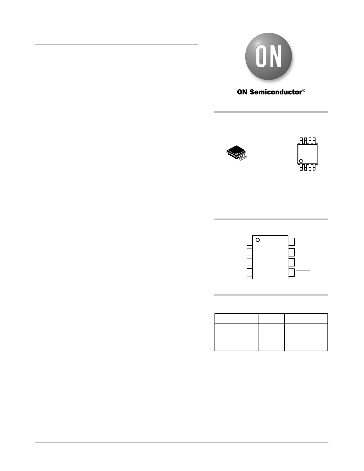
PIN CONNECTIONS
FB 1
LBI 2
LBO 3
REF 4
8 OUT
7 LX
6 GND
5 SHDN
(Top View)
ORDERING INFORMATION
Device
Package
Shipping†
NCP1410DMR2
Micro8 4000 Tape & Reel
NCP1410DMR2G Micro8 4000 Tape & Reel
(Pb-Free)
†For information on tape and reel specifications,
including part orientation and tape sizes, please
refer to our Tape and Reel Packaging Specifications
Brochure, BRD8011/D.
©Ă Semiconductor Components Industries, LLC, 2008
March, 2008 - Rev. 4
1
Publication Order Number:
NCP1410/D
1 page 
NCP1410
TYPICAL OPERATING CHARACTERISTICS
1.212
1.208
1.204
1.2
VOUT = 3.3 V
L = 22 mH
CIN = 10 mF
COUT = 33 mF
CREF = 1.0 mF
TA = 25°C
VIN = 1.8 V
VIN = 2.2 V
1.195
1.193
1.190
1.188
IREF = 0 mA
1.196
1.192
VIN = 3.0 V
1.185
1.183
CREF = 1.0 mF
TA = 25°C
IREF = 2.5 mA
1.188
1.0
10 100
OUTPUT CURRENT, ILOAD/mA
1.180
1000
1.5
2.0 2.5 3.0 3.5 4.0 4.5 5.0 5.5
INPUT VOLTAGE AT OUT PIN, VOUT,/V
Figure 3. Reference Voltage vs. Output Current
Figure 4. Reference Voltage vs. Input Voltage
at OUT pin
1.194
1.192
1.190
1.188
1.186
VOUT = 3.3 V
CREF = 150 nF
IREF = 0 mA
1.184
-40 -20 0 20 40 60
AMBIENT TEMPERATURE, TA/°C
80
100
Figure 5. Reference Voltage vs. Temperature
1.8
1.6
1.4
1.2
P-FET (M2)
1.0
0.8
0.6 N-FET (M1)
0.4
0.2
0
-40
-20 0 20 40 60 80
AMBIENT TEMPERATURE, TA/°C
100
Figure 6. Switch ON Resistance vs. Temperature
1.8
1.7
1.6
1.5
1.4
1.3
1.2
-40
-20 0 20 40 60 80 100
AMBIENT TEMPERATURE, TA/°C
Figure 7. LX Switch Maximum ON Time vs.
Temperature
2.0
1.8 Without Schottky Diode
1.6
1.4
1.2
With Schottky Diode
1.0 (MBR0502)
0.8
0.6
0 20 40 60 80 100 120
OUTPUT LOADING CURRENT, ILOAD/mA
Figure 8. Minimum Startup Battery Voltage vs.
Loading Current
http://onsemi.com
5
5 Page 
NCP1410
Components Placement
Power components, i.e. input capacitor, inductor and
output capacitor, must be placed as close together as
possible. All connecting traces must be short, direct and
thick. High current flowing and switching paths must be
kept away from the feedback (FB, pin 1) terminal to avoid
unwanted injection of noise into the feedback path.
Feedback Network
Feedback of the output voltage must be a separate trace
detached from the power path. External feedback network
must be placed very close to the feedback (FB, pin 1) pin and
sensing the output voltage directly at the anode of the output
capacitor.
TYPICAL APPLICATION CIRCUIT
VIN = 1.8 V to 3.0 V
VBATT
RFB1
355 K
CFB
150 pF
L
22 mH
GND
+ CIN
10 mF/
10 V
RLB1
225 K
RLB2
330 K
RFB2
200 K
1 FB
VOUT 8
2 LBI NCP1410 LX 7
3 LBO
GND 6
4 REF
CREF
150 nF
SHDN 5
VOUT = 3.3 V/250 mA max.
VOUT
RSHDN
560 K
+ COUT
33 mF/
10 V
CSHDN
56 nF
GND
Figure 28. Typical Application Schematic for 2 Alkaline Cells Supply
http://onsemi.com
11
11 Page | ||
| Páginas | Total 13 Páginas | |
| PDF Descargar | [ Datasheet NCP1410.PDF ] | |
Hoja de datos destacado
| Número de pieza | Descripción | Fabricantes |
| NCP1410 | 250 mA Sync-Rect PFM Step-Up DC-DC Converter | ON |
| NCP1411 | Sync-Rect PFM Step-Up DC-DC Converter | ON |
| NCP1417 | 200 mA DC-DC Step-up Converter | ON |
| Número de pieza | Descripción | Fabricantes |
| SLA6805M | High Voltage 3 phase Motor Driver IC. |
Sanken |
| SDC1742 | 12- and 14-Bit Hybrid Synchro / Resolver-to-Digital Converters. |
Analog Devices |
|
DataSheet.es es una pagina web que funciona como un repositorio de manuales o hoja de datos de muchos de los productos más populares, |
| DataSheet.es | 2020 | Privacy Policy | Contacto | Buscar |