|
|
|
PDF NC33395T Data sheet ( Hoja de datos )
| Número de pieza | NC33395T | |
| Descripción | Three-Phase Gate Driver IC | |
| Fabricantes | Motorola Inc | |
| Logotipo | ||
Hay una vista previa y un enlace de descarga de NC33395T (archivo pdf) en la parte inferior de esta página. Total 16 Páginas | ||
|
No Preview Available !
Freescale Semiconductor, Inc.
MOTOROLA
SEMICONDUCTOR TECHNICAL DATA
Document order number: MC33395/D
Rev 2.0, 01/2004
Advance Information
Three-Phase Gate Driver IC
33395
33395T
The 33395 simplifies the design of high-power BLDC motor control design by
combining the gate drive, charge pump, current sense, and protection circuitry
necessary to drive a three-phase bridge configuration of six N-channel power
MOSFETs. Mode logic is incorporated to route a pulse width modulation (PWM)
signal to either the low-side MOSFETs or high-side MOSFETs of the bridge, or
to provide complementary PWM outputs to both the low- and high-sides of the
bridge.
Detection and drive circuitry are also incorporated to control a reverse battery
protection high-side MOSFET switch. PWM frequencies up to 28 kHz are
possible. Built-in protection circuitry prevents damage to the MOSFET bridge as
well as the drive IC and includes overvoltage shutdown, overtemperature
shutdown, overcurrent shutdown, and undervoltage shutdown.
The device is parametrically specified over an ambient temperature range of
-40°C ≤ TA ≤ 125°C and 5.5 V ≤ VIGN ≤ 24 V supply.
Features
• Drives Six N-Channel Low RDS(ON) Power MOSFETs
• Built-In Charge Pump Circuitry
• Built-In Current Sense Comparator and Output Drive Current Limiting
• Built-In PWM Mode Control Logic
• Built-In Circuit Protection
• Designed for Fractional to Integral HP BLDC Motors
• 32-Terminal SOIC Wide Body Surface Mount Package
• 33395 Incorporates a <5.0 µs Shoot-Through Suppression Timer
• 33395T Incorporates a <1.0 µs Shoot-Through Suppression Timer
THREE-PHASE
GATE DRIVER IC
DWB SUFFIX
CASE 1324-02
32-TERMINAL SOICW
ORDERING INFORMATION
Device
Temperature
Range (TA)
Package
MC33395DWB/R2
-40°C to 125°C
MC33395TDWB/R2
32 SOICW
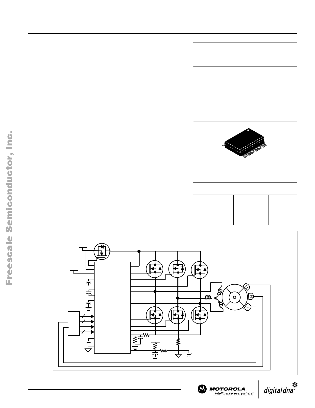
VPWR
33395 Simplified Application Diagram
VDD
3
2
MCU
3
33395
VVGIGDNH
VDD
CP1H
CP1L
CP2H
CP2L
CRES
VIGNP
GDH1
GDH2
GDH3
SRC1
SRC2
SRC3
HSE1–3
MODE0–1
GDL1
PWM
GDL2
LSE1–3
AGND
GDL3
-ISENS
PGND +ISENS
VDD
NH
SS
NH
This document contains certain information on a new product.
Specifications and information herein are subject to change without notice.
© Motorola, Inc. 2004
For More Information On This Product,
Go to: www.freescale.com
1 page 
Freescale Semiconductor, Inc.
MAXIMUM RATINGS
All voltages are with respect to ground unless otherwise noted
VIGN Supply Voltage
Rating
Symbol
VIGN
Value
-15.5 to 40
VIGNP Load Dump Survival
VDD Logic Supply Voltage (Fail Safe)
VIGNPLD
VDD
-0.3 to 65
-0.3 to 7.0
Logic Input Voltage (LSEn, HSEn, PWM, and MODEn)
Start Up Current VIGNP
VIN
IVIGNStartUp
0.3 to 7.0
100
ESD Voltage
Human Body Model (Note 1)
Machine Model (Note 2)
Storage Temperature
Operating Ambient Temperature
Operating Case Temperature
Maximum Junction Temperature
Power Dissipation (TA = 25°C)
VESD1
VESD2
TSTG
TA
TC
TJ
PD
±500
±200
-65 to 160
-40 to 125
-40 to 125
150
1.5
Terminal Soldering Temperature
Thermal Resistance, Junction-to-Ambient
TSOLDER
RθJA
240
65
Notes
1. ESD1 testing is performed in accordance with the Human Body Model (CZAP = 100 pF, RZAP = 1500 Ω).
2. ESD2 testing is performed in accordance with the Machine Model (CZAP = 200 pF, RZAP = 0 Ω).
Unit
VDC
VDC
VDC
VDC
mA
V
°C
°C
°C
°C
W
°C
°C/ W
MOTOROLA ANALOG INTEGRATED CIFRCoUrITMDoErVeICEInDfAoTrAmation On This Product,
Go to: www.freescale.com
33395
5
5 Page 
Freescale Semiconductor, Inc.
Note that the drivers are disabled during an overtemperature
or overvoltage fault. A flip-flop keeps the drive off until the
following PWM cycle. This prevents erratic operation during
fault conditions. The current limit circuit also uses a flip-flop for
latching the drive off until the following PWM cycle.
Note PWM must be toggled after POR, Thermal Limit, or
overvoltage faults to re-enable the gate drivers.
VGDH
The VGDH terminal is used to provide a gate drive signal to a
reverse battery protection MOSFET. If reverse battery
protection is desired, VIGN would be applied to the source of an
external MOSFET, and the drain of the MOSFET would then
deliver a "protected" supply voltage (VIGNP) to the three phase
array of external MOSFETs as well as the supply voltage to the
VIGNP terminal of the IC.
In a reverse polarity event (e.g., an erroneous installation of
the system battery), the VGDH signal will not be supplied to the
external protection MOSFET, and the MOSFET will remain off
and thus prevent reverse polarity from being applied to the load
and the VIGNP supply terminal of the IC.
High-Side Gate Drive Circuits
Outputs GDH1, GDH2, and GDH3 provide the elevated drive
voltage to the high-side external MOSFETs (HS1, HS2, and
HS3; see Figure 3, page 13). These gate drive outputs supply
the peak currents required to turn ON and hold ON the high-
side MOSFETs, as well as turn OFF the MOSFETs. These gate
drive circuits are powered from an internal charge pump, and
therefore compensate for voltage dropped across the load that
is reflected to the source-gate circuits of the high-side
MOSFETs.
Low-Side Gate Drive Circuits
Outputs GDL1, GDL2, and GDL3 provide the drive voltage to
the low-side external MOSFETs (LS1, LS2, and LS3; see
Figure 3). These gate drive outputs supply the peak currents
required to turn ON and hold ON the low-side MOSFETs, as
well as turn OFF the MOSFETs.
VDD Fuse
The VDD supply of the 33395 IC has an internal fuse, which
will blow and set all outputs of the device to OFF, if the VDD
voltage exceeds that stated in the maximum rating section of
the data sheet. When this fuse blows, the device is permanently
disabled.
ISENS Inputs
The +Isens and -Isens terminals are inputs to the internal
current sense comparator. In a typical application, these would
receive a a low-pass filtered voltage derived from a current
sense resistor placed in series with the ground return of the
three-phase output bridge. When triggered by the comparator,
the CL (current limit) bit of the internal error register is set, and
the output gate drive pairs (i.e., GDH1 and GDL1, GDH2 and
GDL2, GDH3 and GDL3), are controlled such that current will
cease flowing through the load (refer to Table 1, Truth Table,
page 12).
Overtemperature and Overvoltage Shutdown
Circuits
Internal monitoring is provided for both over temperature
conditions and over voltage conditions. When any of these
conditions presents itself to the IC, the corresponding internally
set bits of the error register are set, and the output gate drive
pairs (i.e., GDH1 and GDL1, GDH2 and GDL2, GDH3 and
GDL3), are controlled such that current will cease flowing
through the load (refer to Table 1).
LSE and HSE Input Circuits
The low-side enable input terminals (LSE1, LSE2, LSE3)
and high-side enable input terminals (HSE1, HSE2, HSE3) form
the input pairs (HSE1 and LSE1, HSE2 and LSE2, HSE3 and
LSE3) which set the logic states of the output gate drive pairs
(i.e., GDH1 and GDL1, GDH2 and GDL2, GDH3 and GDL3) in
accordance with the logic set forth in the Truth Table (page 12).
Typically these inputs are supplied from an MCU or DSP to
provide the phasing of the currents applied to a brushless dc
motor's stator coils via the output MOSFET pairs.
PWM Input
The pulse width modulation input provides a single input
terminal to accomplish PWM modulation of the output pairs in
accordance with the states of the Mode 0 and Mode 1 inputs as
set forth in the Truth Table (page 12).
Mode Selection Inputs
The mode selection inputs (Mode 0 and Mode 1) determine
the PWM implementation of the output pairs in accordance with
the logic set forth in the Truth Table (page 12). PWM'ing can
thus be set to occur either on the high-side MOSFETs or the
low-side MOSFETs, or can be set to occur on both the high-side
and low-side MOSFETs as "complementary chopping".
Test Terminal
This terminal should be grounded or left floating (i.e., do not
connect it to the printed circuit board). It is used by the
automated test equipment to verify proper operation of the
internal overtemperature shut down circuitry. This terminal is
susceptible to latch-up and therefore may cause erroneous
operation or device failure if connected to external circuitry.
MOTOROLA ANALOG INTEGRATED CIFRCoUrITMDoErVeICEInDfAoTrAmation On This Product,
Go to: www.freescale.com
33395
11
11 Page | ||
| Páginas | Total 16 Páginas | |
| PDF Descargar | [ Datasheet NC33395T.PDF ] | |
Hoja de datos destacado
| Número de pieza | Descripción | Fabricantes |
| NC33395T | Three-Phase Gate Driver IC | Motorola Inc |
| Número de pieza | Descripción | Fabricantes |
| SLA6805M | High Voltage 3 phase Motor Driver IC. |
Sanken |
| SDC1742 | 12- and 14-Bit Hybrid Synchro / Resolver-to-Digital Converters. |
Analog Devices |
|
DataSheet.es es una pagina web que funciona como un repositorio de manuales o hoja de datos de muchos de los productos más populares, |
| DataSheet.es | 2020 | Privacy Policy | Contacto | Buscar |