|
|
|
PDF MAX1604EAI Data sheet ( Hoja de datos )
| Número de pieza | MAX1604EAI | |
| Descripción | Dual-Channel CardBus and PCMCIA Power Switches with SMBus Serial Interface | |
| Fabricantes | Maxim Integrated | |
| Logotipo | ||
Hay una vista previa y un enlace de descarga de MAX1604EAI (archivo pdf) en la parte inferior de esta página. Total 16 Páginas | ||
|
No Preview Available !
19-1085; Rev 1; 10/96
Dual-Channel CardBus and PCMCIA
Power Switches with SMBus™ Serial Interface
________________General Description
The MAX1601/MAX1604 DC power-switching ICs con-
tain a network of low-resistance MOSFET switches that
deliver selectable VCC and VPP voltages to two
CardBus or PC Card host sockets. Key features include
ultra-low-resistance switches, small packaging, soft-
switching action, and compliance with PCMCIA specifi-
cations for 3V/5V switching. 3.3V-only power switching
for fast, 32-bit CardBus applications is supported in two
ways: stiff, low-resistance 3.3V switches allow high 3.3V
load currents (up to 1A); and completely independent
internal charge pumps let the 3.3V switch operate nor-
mally, even if the +5V and +12V supplies are discon-
nected or turned off to conserve power. The internal
charge pumps are regulating types that draw reduced
input current when the VCC switches are static. Also,
power consumption is automatically reduced to 10µA
max when the switches are programmed to high-Z or
GND states over the serial interface, unlike other solu-
tions that may require a separate shutdown-control
input.
Other key features include guaranteed specifications for
output current limit level, and guaranteed specifications
for output rise/fall times (in compliance with PCMCIA
specifications). Reliability is enhanced by thermal-over-
load protection, accurate current limiting, an overcur-
rent-fault flag output, undervoltage lockout, and extra
ESD protection at the VCC/VPP outputs. The SMBus ser-
ial interface is flexible, and can tolerate logic input levels
in excess of the positive supply rail.
The MAX1604 and MAX1601 are identical, except
for the MAX1604’s VY switch, which has roughly three-
times the on-resistance (typically 140mΩ).The
MAX1601/MAX1604 fit two complete CardBus/PCMCIA
switches into a space-saving, narrow (0.2in. or 5mm
wide) SSOP package.
________________________Applications
Desktop Computers Data Loggers
Notebook Computers Digital Cameras
Docking Stations
Printers
Handy-Terminals
PCMCIA Read/Write Drives
Pin Configuration appears on last page.
SMBus is a trademark of Intel Corp.
____________________________Features
o Supports Two CardBus Sockets
o 1A, 0.08Ω Max VY VCC Switch (MAX1601 only)
1A, 0.14Ω Max VX VCC Switch
o Soft Switching for Low Inrush Surge Current
o Overcurrent Protection
o Overcurrent/Thermal-Fault Flag Output
o Thermal Shutdown at Tj = +150°C
o Independent Internal Charge Pumps
o Break-Before-Make Switching Action
o 10µA Max Standby Supply Current
o 5V and 12V Not Required for Low-RDS(ON) 3.3V
Switching
o Complies with PCMCIA 3V/5V Switching
Specifications
o Super-Small, 28-Pin SSOP Package
(0.2in. or 5mm wide)
o System Management Bus (SMBus) Serial
Interface
_______________Ordering Information
PART
MAX1601EAI
MAX1604EAI
TEMP. RANGE
-40°C to +85°C
-40°C to +85°C
PIN-PACKAGE
28 SSOP
28 SSOP
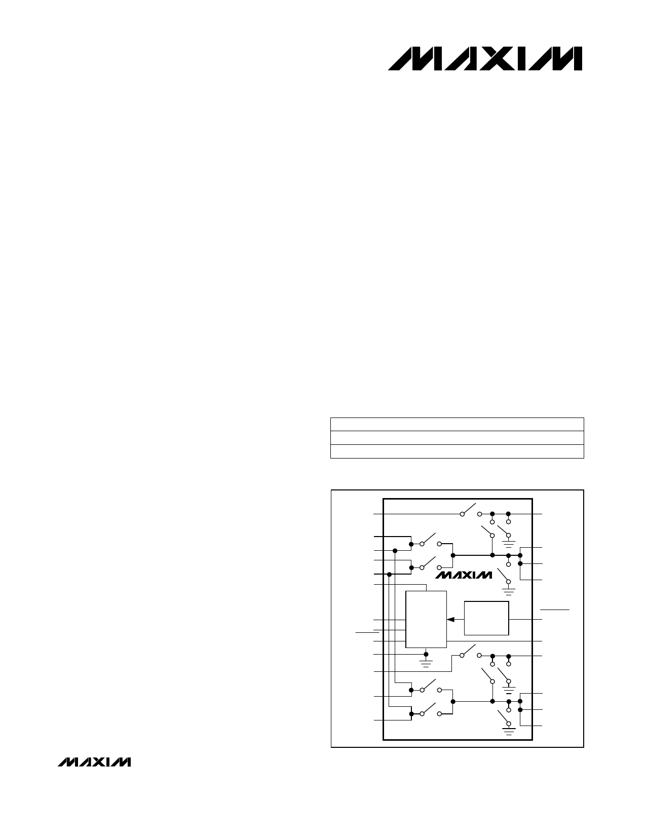
__________Simplified Block Diagram
12IN
VY
VY
VX
VX
VL
SMBCLK
SMBDATA
SMBSUS
GND
12IN
VY
VX
MAX1601/MAX1604
VDD
DECODE
LOGIC
ADDRESS
SELECT
OVERCURRENT
AND
THERMAL
SHUTDOWN
VPPA
VCCA
VCCA
VCCA
SMBALERT
ADR
VPPB
VCCB
VCCB
VCCB
________________________________________________________________ Maxim Integrated Products 1
For free samples & the latest literature: http://www.maxim-ic.com, or phone 1-800-998-8800
1 page 
Dual-Channel CardBus and PCMCIA
Power Switches with SMBus™ Serial Interface
ELECTRICAL CHARACTERISTICS
(VL = VY = 3.3V, VX = 5V, 12INA = 12INB = 12V, TA = -40°C to +85°C, unless otherwise noted.)
PARAMETER
CONDITIONS
POWER-SUPPLY SECTION
Input Voltage Range
VX, VY or VL
12INA, 12INB
VL falling edge, hysteresis = 1%
12IN falling edge
Undervoltage Lockout Threshold
12IN rising edge
VX, VY falling edge
Standby Supply Current
VX or VY, all switches 0V or high-Z,
control inputs = 0V or VL
MIN TYP MAX UNITS
3.0 5.5
V
11 13
2.3 2.9
1.8
V
5 10
1.4 2.9
15 µA
VY Quiescent Supply Current
Any combination of VY switches on,
control inputs = 0V or VL, no VCC loads
100 µA
VX Quiescent Supply Current
Any combination of VX switches on,
control inputs = 0V or high-Z, no VCC loads
100 µA
12IN_ Standby Supply Current
12INA tied to 12INB, all switches 0V or high-Z,
control inputs = 0V or VL
15 µA
12IN_ Quiescent Supply Current
12INA tied to 12INB, VPPA and VPPB 12V switches on,
control inputs = 0V or VL, no VPP loads
100 µA
VL Standby Supply Current
All switches 0V or high-Z, control inputs = 0V or VL
15 µA
VL Quiescent Supply Current
Any combination of switches on
INTERFACE AND LOGIC SECTION
SMBALERT Output Low Voltage ISINK = 1mA, low state
Logic Input Low Voltage
SMBCLK, SMBDATA, SMBSUS
Logic Input High Voltage
SMBCLK, SMBDATA, SMBSUS
Logic Output Low Voltage
SMBDATA, ISINK = 4mA
ADR Input Low Voltage
ADR Input High Voltage
150 µA
0.4 V
0.8 V
2.2 V
0.4 V
0.6 V
1.5 V
_______________________________________________________________________________________ 5
5 Page 
Dual-Channel CardBus and PCMCIA
Power Switches with SMBus™ Serial Interface
_______________Detailed Description
The MAX1601/MAX1604 power-switching ICs contain a
network of low-resistance MOSFET switches that deliver
selectable VCC and VPP voltages to two Cardbus or
PC Card host sockets. The MAX1601/MAX1604 differ
only in the VY switch on-resistance. Figure 1 is the
detailed block diagram.
The power-input pins (VY, VX, 12IN_) are completely
independent. Low inrush current is guaranteed by con-
trolled switch rise times. VCC’s 100µs minimum output
rise time is 100% tested with a 1µF capacitive load, and
VPP’s 1ms minimum rise time is guaranteed with a 0.1µF
load. These respective capacitive loads are chosen as
worst-case card-insertion parameters. The internal
switching control allows VCC and VPP rise times to be
controlled, and makes them nearly independent of resis-
tive and capacitive loads (see rise-time photos in the
Typical Operating Characteristics). Fall times are a
function of loading, and are compensated by internal
circuitry.
Power savings is automatic: internal charge pumps draw
very low current when the VCC switches are static.
Standby mode reduces switch supply current to 1µA.
Driving the VL pin low with an external logic gate (master
shutdown) reduces total supply current to1µA (Figure 2).
Operating Modes
The MAX1601/MAX1604 have three operating modes:
normal, standby, and shutdown. Normal mode supplies
the selected outputs with their appropriate supply volt-
ages. Standby mode places all switches at ground, high
impedance, or a combination of the two. Shutdown mode
turns all switches off, and puts the VCC and VPP outputs
into a high-impedance state. Pull VL low to enter shutdown
mode. To ensure a 0.05V/µs fall rate on VL, use a 1kΩ
series resistor and a 0.1µF capacitor to ground (Figure 2).
Overcurrent Protection
Peak detecting circuitry protects both the VCC and
VPP switches against overcurrent conditions. When
current through any switch exceeds the internal current
limit (4A for VCC switches and 200mA for VPP switch-
es), the switch turns off briefly, then turns on again at
the controlled rise rate. If the overcurrent condition
lasts more than 2µs, the SMBALERT output latches
MASTER
SHUTDOWN
74HC04
1k
0.1µF
3.3V
VY VPPA
VL VCCA
MAX1601
MAX1604
VPPB
VCCB
TO
SOCKETS
A AND B
Figure 2. Master Shutdown Circuit
low. A continuous short-circuit condition results in a
pulsed output current until thermal shutdown is
reached. SMBALERT is open-drain and requires an
external pull-up resistor.
Thermal Shutdown
If the IC junction temperature rises above +150°C, the
thermal shutdown circuitry opens all switches, including
the GND switches, and SMBALERT is pulled low. When
the temperature falls below +130°C, the switches turn
on again at the controlled rise rate. If the overcurrent
condition remains, the part cycles between thermal
shutdown and overcurrent.
Undervoltage Lockout
If the VX or VY switch input voltage drops below 1.5V,
the associated switch turns off and SMBALERT goes
low. For example, if VY is 3.3V and VX is 0V, and if the
interface controller selects VY, the VCCA output will be
3.3V. If VX is selected, VCCA changes to a high-imped-
ance output and SMBALERT goes low.
When a voltage is initially applied to 12IN_, it must be
greater than 8V to allow the switch to operate.
Operation continues until the voltage falls below 2V (the
VPP output is high impedance).
When VL drops to less than 2.3V, all switches are
turned off and the VCC and VPP outputs are high
impedance.
______________________________________________________________________________________ 11
11 Page | ||
| Páginas | Total 16 Páginas | |
| PDF Descargar | [ Datasheet MAX1604EAI.PDF ] | |
Hoja de datos destacado
| Número de pieza | Descripción | Fabricantes |
| MAX1604EAI | Dual-Channel CardBus and PCMCIA Power Switches with SMBus Serial Interface | Maxim Integrated |
| Número de pieza | Descripción | Fabricantes |
| SLA6805M | High Voltage 3 phase Motor Driver IC. |
Sanken |
| SDC1742 | 12- and 14-Bit Hybrid Synchro / Resolver-to-Digital Converters. |
Analog Devices |
|
DataSheet.es es una pagina web que funciona como un repositorio de manuales o hoja de datos de muchos de los productos más populares, |
| DataSheet.es | 2020 | Privacy Policy | Contacto | Buscar |