|
|
|
PDF MAX1595 Data sheet ( Hoja de datos )
| Número de pieza | MAX1595 | |
| Descripción | Regulated 3.3V/5.0V Step-Up/Step-Down Charge Pump | |
| Fabricantes | Maxim Integrated | |
| Logotipo | ||
Hay una vista previa y un enlace de descarga de MAX1595 (archivo pdf) en la parte inferior de esta página. Total 8 Páginas | ||
|
No Preview Available !
19-2107; Rev 1; 8/02
Regulated 3.3V/5.0V Step-Up/Step-Down
Charge Pump
General Description
The MAX1595 charge-pump regulator generates either
3.3V or 5V from a 1.8V to 5.5V input. The unique control
architecture allows the regulator to step up or step
down the input voltage to maintain output regulation.
The 1MHz switching frequency, combined with a
unique control scheme, allows the use of a ceramic
capacitor as small as 1µF for 125mA of output current.
The complete regulator requires three external capaci-
tors—no inductor is needed. The MAX1595 is specifi-
cally designed to serve as a high-power, high-
efficiency auxiliary supply in applications that demand
a compact design. The MAX1595 is offered in space-
saving 8-pin µMAX and high-power 12-pin thin QFN
packages.
Applications
White LED Power
Flash Memory Supplies
Battery-Powered Applications
Miniature Equipment
PCMCIA Cards
3.3V to 5V Local Conversion Applications
Backup-Battery Boost Converters
3V to 5V GSM SIMM Cards
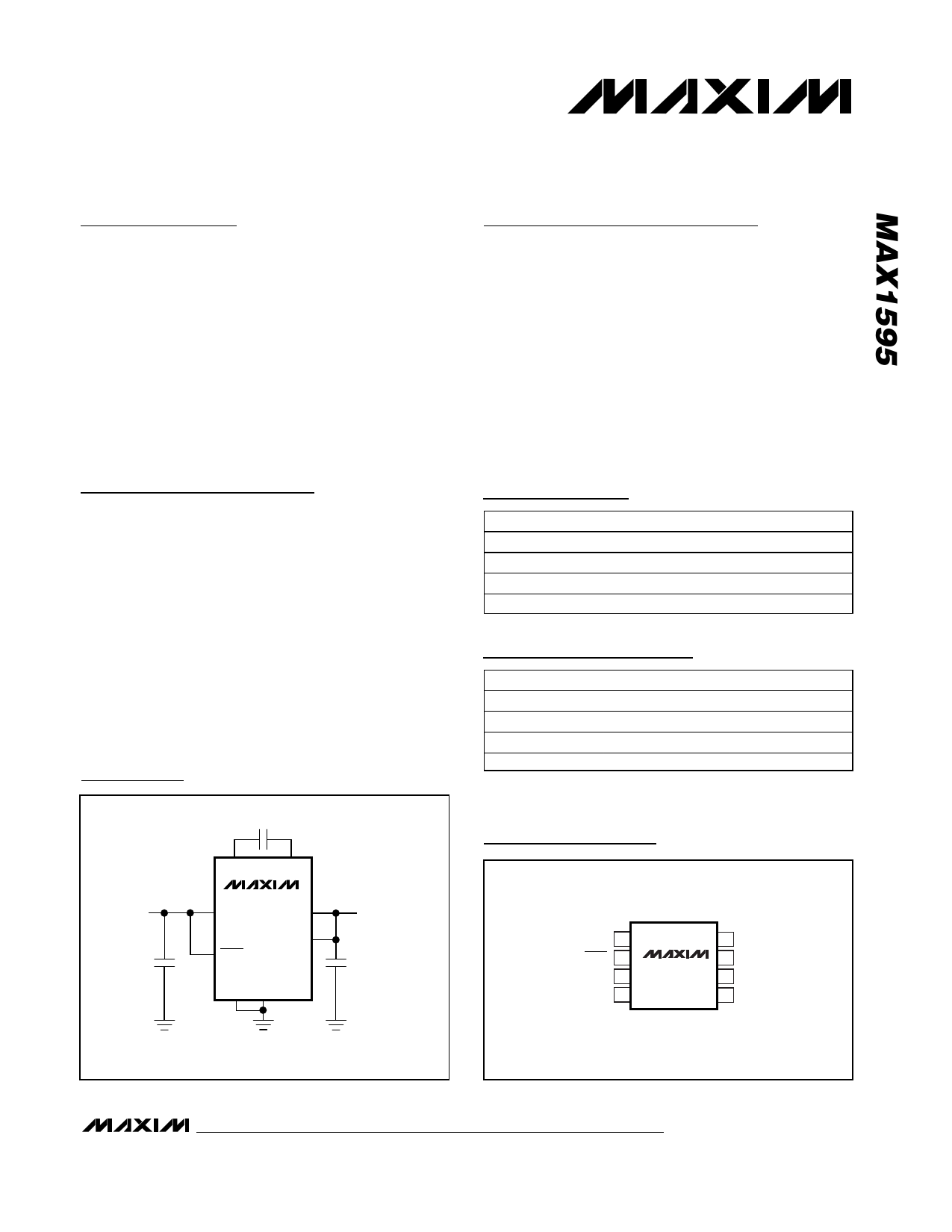
Typical Operating Circuit
Features
o Ultra-Small: Requires Only Three Ceramic
Capacitors
o No Inductors Required
o Up to 125mA Output Current
o Regulated ±3% Output Voltage
o 1MHz Switching Frequency
o 1.8V to 5.5V Input Voltage
o 220µA Quiescent Current
o 0.1µA Shutdown Current
o Load Disconnect in Shutdown
Ordering Information
PART
MAX1595EUA33
MAX1595ETC33
MAX1595EUA50
MAX1595ETC50
TEMP RANGE
-40°C to +85°C
-40°C to +85°C
-40°C to +85°C
-40°C to +85°C
PIN-PACKAGE
8 µMAX
12 Thin QFN
8 µMAX
12 Thin QFN
Selector Guide
PART
VOUT *
TOP MARK
MAX1595EUA33
3.3V
—
MAX1595ETC33
3.3V
AAAP
MAX1595EUA50
5.0V
—
MAX1595ETC50
5.0V
AAAM
*Contact factory for other fixed-output voltages from 2.7V to 5.0V.
INPUT
CXN CXP
MAX1595
IN OUT
SHDN
AOUT
PGND GND
OUTPUT
Pin Configurations
TOP VIEW
AOUT 1
SHDN 2
IN 3
GND 4
MAX1595
µMAX
8 OUT
7 CXP
6 CXN
5 PGND
Pin Configurations continued at end of data sheet.
Maxim Integrated Products 1
For pricing delivery, and ordering information please contact Maxim/Dallas Direct! at
1-888-629-4642, or visit Maxim’s website at www.maxim-ic.com.
1 page 
Regulated 3.3V/5.0V Step-Up/Step-Down
Charge Pump
exceeds the available battery voltage, the use of a
charge pump such as the MAX1595 provides high effi-
ciency, small size, and constant light output with chang-
ing battery voltages. If the output is used only to light
LEDs, the output capacitor can be greatly reduced. The
frequency modulation of the LED intensity is not dis-
cernible to the human eye, and the smaller capacitor
saves both size and cost.
Adding two Schottky diodes and two capacitors imple-
ments a tripler and allows the MAX1595_ _ _50 to regu-
late a current of 75mA with a supply voltage as low as
2.3V (Figure 3).
Capacitor Selection
The MAX1595 requires only three external capacitors
(Figure 4). Their values are closely linked to the output
current capacity, oscillator frequency, output noise con-
tent, and mode of operation.
Generally, the transfer capacitor (CX) will be the smallest,
and the input capacitor (CIN) is twice as large as CX.
Higher switching frequencies allow the use of the smaller
CX and CIN. The output capacitor (COUT) can be any-
where from 5-times to 50-times larger than CX. Table 1
shows recommended capacitor values.
In addition, the following equation approximates output
ripple:
VRIPPLE ≅ IOUT / (2 x fOSC x COUT)
Table 2 lists the manufacturers of recommended capaci-
tors. Ceramic capacitors will provide the lowest ripple
due to their typically lower ESR.
Power Dissipation
The power dissipated in the MAX1595 depends on out-
put current and is accurately described by:
PDISS = IOUT (2VIN - VOUT)
PDISS must be less than that allowed by the package
rating.
Layout Considerations
All capacitors should be soldered in close proximity to
the IC. Connect ground and power ground through a
short, low-impedance trace. The input supply trace
should be as short as possible. Otherwise, an additional
input supply filter capacitor (tantalum or electrolytic) may
be required.
VIN
CIN = 1µF
CX = 0.1µF
CXP CXN
MAX1595_ _ _50
IN OUT
SHDN
AOUT
PGND GND
COUT =
0.47µF
100Ω
100Ω
100Ω
Figure 2. White LED Bias Supply
INPUT
2.3V
1µF
IN
SHDN
AOUT
OUT
MAX1595_ _ _50
CXP
PGND GND CXN
OUTPUT
REGULATED 5V
1µF 0.22µF 1µF 75mA
0.22µF
Figure 3. Regulated Voltage Tripler
ON
OFF
IN
CIN
1µF
2
SHDN
3
IN
MAX1595
PGND GND
54
7
CXP
CXN 6
8
OUT
1
AOUT
CX
0.22µF
OUT
COUT
1µF
Figure 4. Standard Operating Circuit
_______________________________________________________________________________________ 5
5 Page | ||
| Páginas | Total 8 Páginas | |
| PDF Descargar | [ Datasheet MAX1595.PDF ] | |
Hoja de datos destacado
| Número de pieza | Descripción | Fabricantes |
| MAX159 | +2.7V / Low-Power / 2-Channel / 108ksps / Serial 10-Bit ADCs in 8-Pin UMAX | Maxim Integrated |
| MAX1595 | Regulated 3.3V/5.0V Step-Up/Step-Down Charge Pump | Maxim Integrated |
| MAX1598 | Low-Noise / Low-Dropout / 200mA Linear Regulator | Maxim Integrated |
| MAX1599 | High-Efficiency / 26V Step-Up Converters for Two to Six White LEDs | Maxim Integrated |
| Número de pieza | Descripción | Fabricantes |
| SLA6805M | High Voltage 3 phase Motor Driver IC. |
Sanken |
| SDC1742 | 12- and 14-Bit Hybrid Synchro / Resolver-to-Digital Converters. |
Analog Devices |
|
DataSheet.es es una pagina web que funciona como un repositorio de manuales o hoja de datos de muchos de los productos más populares, |
| DataSheet.es | 2020 | Privacy Policy | Contacto | Buscar |