|
|
|
PDF MAX1242 Data sheet ( Hoja de datos )
| Número de pieza | MAX1242 | |
| Descripción | +2.7V to %.25V / Low-Power / 10-Bit Serial ADCs in SO-8 | |
| Fabricantes | Maxim Integrated | |
| Logotipo | ||
Hay una vista previa y un enlace de descarga de MAX1242 (archivo pdf) en la parte inferior de esta página. Total 12 Páginas | ||
|
No Preview Available !
19-1156; Rev 2; 6/98
+2.7V to +5.25V, Low-Power, 10-Bit
Serial ADCs in SO-8
__________________General Description
The MAX1242/MAX1243 are low-power, 10-bit analog-
to-digital converters (ADCs) available in 8-pin pack-
ages. They operate with a single +2.7V to +5.25V
supply and feature a 7.5µs successive-approximation
ADC, a fast track/hold (1.5µs), an on-chip clock, and a
high-speed, 3-wire serial interface.
Power consumption is only 3mW (VDD = 3V) at the
73ksps maximum sampling speed. A 2µA shutdown
mode reduces power at slower throughput rates.
The MAX1242 has an internal 2.5V reference, while the
MAX1243 requires an external reference. The MAX1243
accepts signals from 0V to VREF, and the reference
input range includes the positive supply rail. An exter-
nal clock accesses data from the 3-wire interface,
which connects directly to standard microcontroller I/O
ports. The interface is compatible with SPI™, QSPI™,
and Microwire™.
Excellent AC characteristics and very low power com-
bined with ease of use and small package size make
these converters ideal for remote-sensor and data-
acquisition applications, or for other circuits with
demanding power consumption and space require-
ments. The MAX1242/MAX1243 are available in 8-pin
DIP and SO packages.
Applications
Portable Data Logging Process Control Monitoring
Test Equipment
Temperature Measurement
Isolated Data Acquisition
________________________________Features
o +2.7V to +5.25V Single-Supply Operation
o 10-Bit Resolution
o Internal 2.5V Reference (MAX1242)
o Small Footprint: 8-Pin DIP and SO Packages
o Low Power: 3.7mW (73ksps, MAX1242)
3mW (73ksps, MAX1243)
66µW (1ksps, MAX1243)
5µW (power-down mode)
o Internal Track/Hold
o SPI™/QSPI™/Microwire™ 3-Wire Serial Interface
o Pin-Compatible 12-Bit Upgrades:
MAX1240/MAX1241
_________________Ordering Information
PART
MAX1242ACPA
TEMP. RANGE
PIN-
PACKAGE
0°C to +70°C 8 Plastic DIP
INL
(LSB)
±1/2
MAX1242BCPA
MAX1242ACSA
0°C to +70°C
0°C to +70°C
8 Plastic DIP
8 SO
±1
±1/2
MAX1242BCSA 0°C to +70°C
MAX1242AEPA -40°C to +85°C
8 SO
8 Plastic DIP
±1
±1/2
MAX1242BEPA -40°C to +85°C 8 Plastic DIP ±1
Ordering Information continued at end of data sheet.
Note: Order the MAX1242A in place of the MAX1242C. Order the
MAX1242B in place of the MAX1242D.
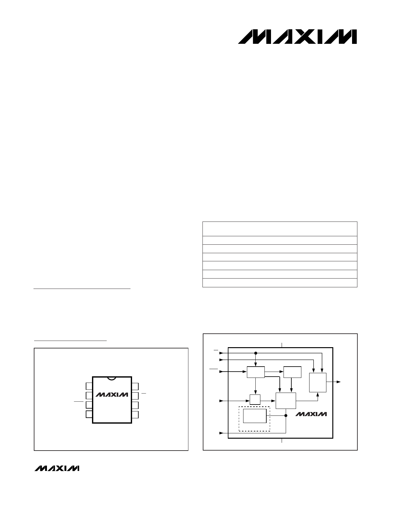
________________Functional Diagram
TOP VIEW
Pin Configuration
VDD 1
AIN 2
SHDN 3
REF 4
MAX1242
MAX1243
8 SCLK
7 CS
6 DOUT
5 GND
DIP/SO
CS
SCLK
7
8
SHDN 3
AIN 2
4
REF
VDD
1
CONTROL
LOGIC
T/H
2.5V
REFERENCE
MAX1242 ONLY
INT
CLOCK
10-BIT
SAR
OUTPUT
SHIFT
REGISTER
MAX1242
MAX1243
5
GND
SPI and QSPI are trademarks of Motorola, Inc. Microwire is a trademark of National Semiconductor Corp.
6
DOUT
________________________________________________________________ Maxim Integrated Products 1
For free samples & the latest literature: http://www.maxim-ic.com, or phone 1-800-998-8800.
For small orders, phone 408-737-7600 ext. 3468.
1 page 
+2.7V to +5.25V, Low-Power, 10-Bit
Serial ADCs in SO-8
__________________________________________Typical Operating Characteristics
(VDD = +3.0V, VREF = 2.5V, fSCLK = 2.1MHz, CLOAD = 20pF, TA = +25°C, unless otherwise noted.)
SUPPLY CURRENT
vs. SUPPLY VOLTAGE
2.00
1.75 CLOAD = 20pF CLOAD = 50pF
1.50 MAX1242
1.25
MAX1243
1.00
CLOAD = 50pF
CLOAD = 20pF
0.75
RL = ∞
CODE = 1010101000
0.50
2.25 2.75 3.25 3.75 4.25 4.75 5.25
SUPPLY VOLTAGE (V)
SUPPLY CURRENT vs. TEMPERATURE
1.3
1.2 MAX1242
1.1
1.0
MAX1243
0.9
RLOAD = ∞
CODE = 1010101000
0.8
-60 -20 20
60
TEMPERATURE (°C)
100
140
INTEGRAL NONLINEARITY
vs. SUPPLY VOLTAGE
0.30
0.25
0.20
0.15
0.10 MAX1242
0.05
MAX1243
0
2.25
2.75 3.25 3.75 4.25 4.75
SUPPLY VOLTAGE (V)
5.25
SHUTDOWN SUPPLY CURRENT
vs. SUPPLY VOLTAGE
4.0
3.5 MAX1242/MAX1243
3.0
2.5
2.0
1.5
1.0
0.5
0
2.25
2.75 3.25 3.75 4.25 4.75
SUPPLY VOLTAGE (V)
5.25
SHUTDOWN CURRENT
vs. TEMPERATURE
3.00
2.75
2.50
2.25
2.00
1.75
1.50
1.25
1.00
-60
-20 20 60 100
TEMPERATURE (°C)
140
INTEGRAL NONLINEARITY
vs. TEMPERATURE
0.30
VDD = 2.7V
0.25
0.20
0.15
0.10
MAX1242
0.05
MAX1243
0
-60 -40 -20 0 20 40 60 80 100 120 140
TEMPERATURE (°C)
2.5015
2.5010
INTERNAL REFERENCE VOLTAGE
vs. SUPPLY VOLTAGE
MAX1242
2.5005
2.5000
2.4995
2.4990
2.4985
2.25
2.75 3.25
SUPPLY VOLTAGE (V)
3.75
INTERNAL REFERENCE VOLTAGE
vs. TEMPERATURE
2.501
2.500
2.499
MAX1242
VDD = 5V
VDD = 3.6V
2.498
VDD = 2.7V
2.497
2.496
2.495
2.494
-60 -40 -20 0 20 40 60 80 100 120 140
TEMPERATURE (°C)
INTEGRAL NONLINEARITY
vs. CODE
0.15
0.10
0.05
0
-0.05
-0.10
-0.15
0
256 512 768 1024
CODE
_______________________________________________________________________________________ 5
5 Page 
+2.7V to +5.25V, Low-Power, 10-Bit
Serial ADCs in SO-8
SCLK
CS
DOUT
tCONV
EOC
1ST BYTE READ
D9 D8 D7 D6 D5 D4 D3
MSB
Figure 12. SPI/Microwire Serial-Interface Timing (CPOL = CPHA = 0)
D2
2ND BYTE READ
D1 D0 S1
LSB
S0
HIGH-Z
SCLK
CS
DOUT
tCONV
EOC
D9 D8 D7 D6 D5 D4 D3 D2 D1 D0 S1 S0
MSB LSB
HIGH-Z
Figure 13. QSPI Serial-Interface Timing (CPOL = CPHA = 0)
If a serial interface is available, set the CPU’s serial
interface in master mode so the CPU generates the ser-
ial clock. Choose a clock frequency up to 2.1MHz.
1) Use a general-purpose I/O line on the CPU to pull CS
low. Keep SCLK low.
2) Wait the maximum conversion time specified before
activating SCLK. Alternatively, look for a DOUT rising
edge to determine the end of conversion.
3) Activate SCLK for a minimum of 11 clock cycles. The
first falling clock edge produces the MSB of the
DOUT conversion. DOUT output data transitions on
SCLK’s falling edge and is available in MSB-first for-
mat. Observe the SCLK-to-DOUT valid timing char-
acteristic. Data can be clocked into the µP on
SCLK’s rising edge.
4) Pull CS high at or after the 11th falling clock edge. If
CS remains low, the two sub-bits and trailing zeros
are clocked out after the LSB.
5) With CS = high, wait the minimum specified time, tCS,
before initiating a new conversion by pulling CS low.
If a conversion is aborted by pulling CS high before
the conversion’s end, wait the minimum acquisition
time, tACQ, before starting a new conversion.
Data can be output in two bytes or continuously, as
shown in Figures 8a and 8b. The bytes contain the
result of the conversion padded with one leading 1, two
sub-bits, and trailing 0s if SCLK is still active with CS
kept low.
SPI and Microwire
When using SPI or QSPI, set CPOL = 0 and CPHA = 0.
Conversion begins with a CS falling edge. DOUT goes
low, indicating a conversion is in progress. Wait until
DOUT goes high or until the maximum specified 7.5µs
conversion time elapses. Two consecutive 1-byte reads
are required to get the full 10+2 bits from the ADC.
DOUT output data transitions on SCLK’s falling edge
and is clocked into the µP on SCLK’s rising edge.
The first byte contains a leading 1, and seven bits of
conversion result. The second byte contains the remain-
ing three bits, two sub-bits, and three trailing zeros. See
Figure 11 for connections and Figure 12 for timing.
QSPI
Set CPOL = CPHA = 0. Unlike SPI, which requires two
1-byte reads to acquire the 10 bits of data from the ADC,
QSPI allows the minimum number of clock cycles neces-
sary to clock in the data. The MAX1242/MAX1243 require
11 clock cycles from the µP to clock out the 10 bits of
data. Additional clock cycles clock out the two sub-bits
followed by trailing zeros (Figure 13). The maximum clock
frequency to ensure compatibility with QSPI is 2.097MHz.
Layout and Grounding
For best performance, use printed circuit boards. Wire-
wrap boards are not recommended. Board layout
should ensure that digital and analog signal lines are
separated from each other. Do not run analog and digi-
tal (especially clock) lines parallel to one another, or
digital lines underneath the ADC package.
______________________________________________________________________________________ 11
11 Page | ||
| Páginas | Total 12 Páginas | |
| PDF Descargar | [ Datasheet MAX1242.PDF ] | |
Hoja de datos destacado
| Número de pieza | Descripción | Fabricantes |
| MAX1240 | 12-Bit Serial ADCs | Maxim Integrated |
| MAX1241 | 12-Bit Serial ADCs | Maxim Integrated |
| MAX1242 | +2.7V to %.25V / Low-Power / 10-Bit Serial ADCs in SO-8 | Maxim Integrated |
| MAX1243 | +2.7V to %.25V / Low-Power / 10-Bit Serial ADCs in SO-8 | Maxim Integrated |
| Número de pieza | Descripción | Fabricantes |
| SLA6805M | High Voltage 3 phase Motor Driver IC. |
Sanken |
| SDC1742 | 12- and 14-Bit Hybrid Synchro / Resolver-to-Digital Converters. |
Analog Devices |
|
DataSheet.es es una pagina web que funciona como un repositorio de manuales o hoja de datos de muchos de los productos más populares, |
| DataSheet.es | 2020 | Privacy Policy | Contacto | Buscar |