|
|
|
PDF M93S56 Data sheet ( Hoja de datos )
| Número de pieza | M93S56 | |
| Descripción | 4Kbit / 2Kbit and 1Kbit 16-bit wide MICROWIRE Serial Access EEPROM with Block Protection | |
| Fabricantes | ST Microelectronics | |
| Logotipo | ||
Hay una vista previa y un enlace de descarga de M93S56 (archivo pdf) en la parte inferior de esta página. Total 30 Páginas | ||
|
No Preview Available !
M93S66, M93S56
M93S46
4Kbit, 2Kbit and 1Kbit (16-bit wide)
MICROWIRE Serial Access EEPROM with Block Protection
FEATURES SUMMARY
s Industry Standard MICROWIRE Bus
s Single Supply Voltage:
– 4.5V to 5.5V for M93Sx6
– 2.5V to 5.5V for M93Sx6-W
– 1.8V to 5.5V for M93Sx6-R
s Single Organization: by Word (x16)
s Programming Instructions that work on: Word or
Entire Memory
s Self-timed Programming Cycle with Auto-Erase
s User Defined Write Protected Area
s Page Write Mode (4 words)
s Ready/Busy Signal During Programming
s Speed:
– 1MHz Clock Rate, 10ms Write Time (Current
product, identified by process identification
letter F or M)
– 2MHz Clock Rate, 5ms Write Time (New
Product, identified by process identification
letter W)
s Sequential Read Operation
s Enhanced ESD/Latch-Up Behavior
s More than 1 Million Erase/Write Cycles
s More than 40 Year Data Retention
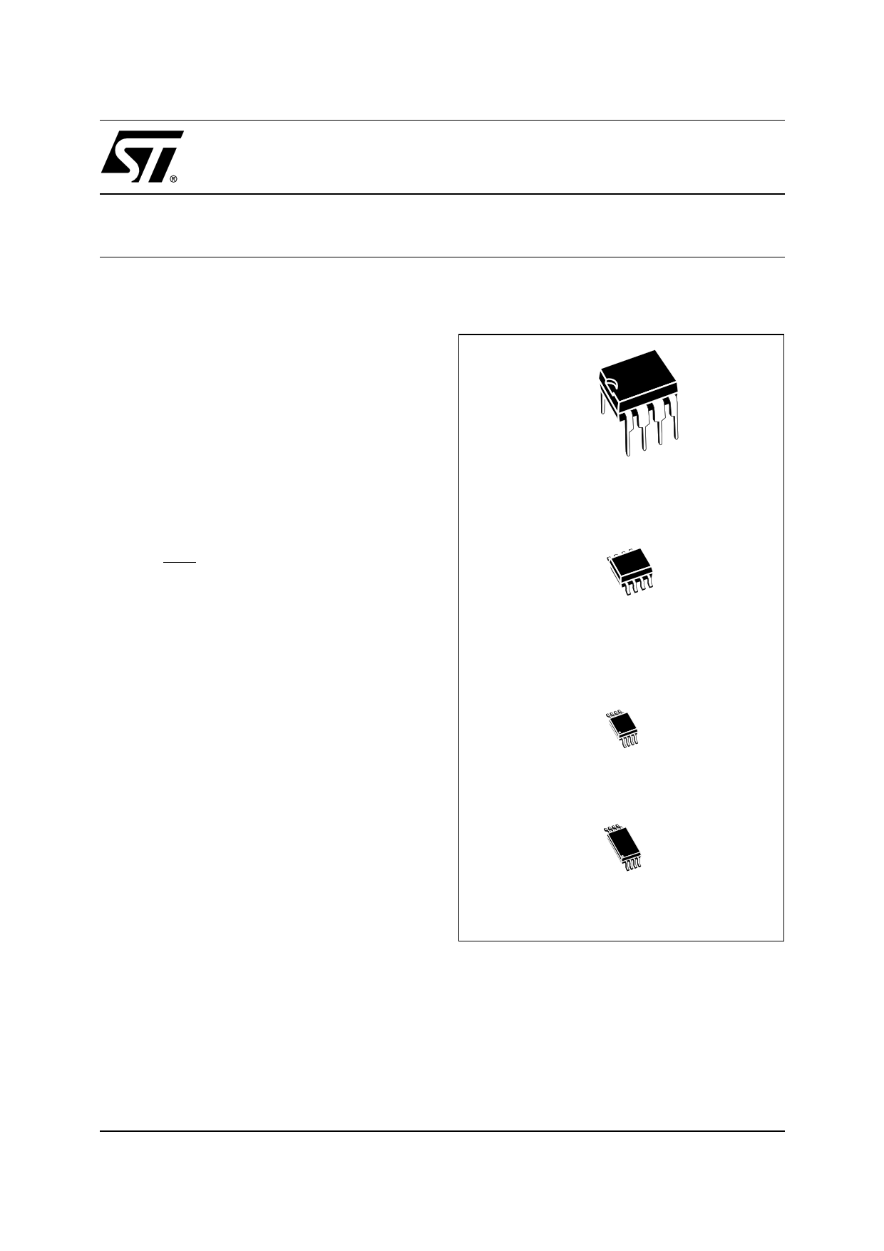
Figure 1. Packages
8
1
PDIP8 (BN)
8
1
SO8 (MN)
150 mil width
TSSOP8 (DS)
3x3mm body size
TSSOP8 (DW)
169 mil width
May 2003
1/32
1 page 
M93S66, M93S56, M93S46
Table 3. Instruction Set for the M93S66, M93S56
Instruction
Description
W
PRE
Start
bit
Op-
Code
Address1,2
Data
Required
Clock
Cycles
Additional
Comments
READ
Read Data
from Memory
X
0
1
10
A7-A0 Q15-Q0
WRITE
Write Data to
Memory
1
0
1
01
A7-A0 D15-D0
Write is executed if
27
the address is not
inside the
Protected area
PAWRITE
Page Write to
Memory
1
0
1
11
A7-A0
Nx
D15-D0
11 + N x 16
Write is executed if
all the N
addresses are not
inside the
Protected area
WRAL
Write All
Memory
with same
Data
Write all data if the
1 0 1 00 01XXXXXX D15-D0 27 Protection
Register is cleared
WEN
Write Enable 1 0 1 00 11XXXXXX
11
WDS
Write Disable X 0 1 00 00XXXXXX
11
PRREAD
Protection
Register Read
X
1
1
10
XXXXXXXX
Q7-Q0
+ Flag
Data Output =
Protection
Register content +
Protection Flag bit
PRWRITE
Protection
Register Write
1
1
1
01
A7-A0
Data above
11
specified address
A7-A0 are
protected
PRCLEAR
Protection
Register Clear
1
1
1
11 11111111
Protect Flag is also
11 cleared (cleared
Flag = 1)
PREN
Protection
Register
Enable
1 1 1 00 11XXXXXX
11
PRDS
Protection
Register
Disable
1 1 1 00 00000000
11
OTP bit is set
permanently
Note: 1. X = Don’t Care bit.
2. Address bit A7 is not decoded by the M93S56.
5/32
5 Page 
Figure 7. PRCLEAR and PRDS Sequences
Protect
Register
CLEAR
PRE
W
M93S66, M93S56, M93S46
S
CHECK
STATUS
D
111
111
Q
Protect
Register
DISABLE
PRE
W
ADDR
OP
CODE
BUSY
READY
S
CHECK
STATUS
D
100
000
Q
ADDR
OP
CODE
BUSY
READY
Note: For the meanings of An, Xn and Dn, please see Table 2 and Table 3.
AI00892C
11/32
11 Page | ||
| Páginas | Total 30 Páginas | |
| PDF Descargar | [ Datasheet M93S56.PDF ] | |
Hoja de datos destacado
| Número de pieza | Descripción | Fabricantes |
| M93S56 | 4Kbit / 2Kbit and 1Kbit 16-bit wide MICROWIRE Serial Access EEPROM with Block Protection | ST Microelectronics |
| M93S56-125 | MICROWIRE serial EEPROM | STMicroelectronics |
| M93S56-W | MICROWIRE bus EEPROM | STMicroelectronics |
| Número de pieza | Descripción | Fabricantes |
| SLA6805M | High Voltage 3 phase Motor Driver IC. |
Sanken |
| SDC1742 | 12- and 14-Bit Hybrid Synchro / Resolver-to-Digital Converters. |
Analog Devices |
|
DataSheet.es es una pagina web que funciona como un repositorio de manuales o hoja de datos de muchos de los productos más populares, |
| DataSheet.es | 2020 | Privacy Policy | Contacto | Buscar |