|
|
|
PDF M6MGT166S2BWG Data sheet ( Hoja de datos )
| Número de pieza | M6MGT166S2BWG | |
| Descripción | CMOS 3.3V-ONLY FLASH MEMORY & CMOS SRAM Stacked-CSP | |
| Fabricantes | Mitsubishi | |
| Logotipo | ||
Hay una vista previa y un enlace de descarga de M6MGT166S2BWG (archivo pdf) en la parte inferior de esta página. Total 30 Páginas | ||
|
No Preview Available !
MITSUBISHI LSIs
M6MGB/T166S2BWG
16,777,216-BIT (1,048,576 -WORD BY 16-BIT ) CMOS
3.3V-ONLY FLASH MEMORY &
2,097,152-BIT (131,072-WORD BY 16-BIT) CMOS SRAM
Stacked-CSP (Chip Scale Package)
DESCRIPTION
FEATURES
The MITSUBISHI M6MGB/T166S2BWG is a Stacked Chip
Scale Package (S-CSP) that contents 16M-bits flash
memory and 2M-bits Static RAM in a 72-pin S-CSP.
16M-bits Flash memory is a 1,048,576 words, 3.3V-only,
and high performance non-volatile memory fabricated by
CMOS technology for the peripheral circuit and
DINOR(DIvided bit-line NOR) architecture for the memory
cell.
2M-bits SRAM is a 131,072words unsynchronous SRAM
fabricated by silicon-gate CMOS technology.
M6MGB/T166S2BWG is suitable for the application of the
mobile-communication-system to reduce both the mount
space and weight .
• Access time
Flash Memory
90ns (Max.)
SRAM
85ns (Max.)
• Supply voltage
Vcc=2.7 ~ 3.6V
• Ambient temperature
I version
Ta=-40 ~ 85°C
• Package : 72-pin S-CSP , 0.8mm ball pitch
APPLICATION
Mobile communication products
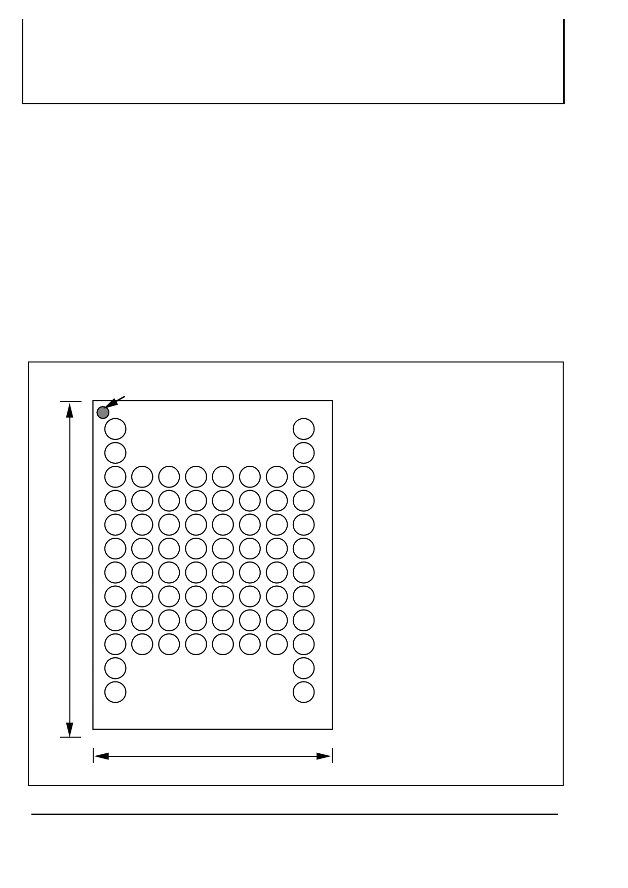
PIN CONFIGURATION (TOP VIEW)
INDEX (Laser Marking)
1234 5678
A NC
NC
B NC
NC
C DU F-A18 S-LB# F-WP# GND F-WE# A16 NC
F-
D A5 F-A17 S-UB# NC F-RP# RY/BY# A8 A11
E A4 A7 S-OE# F-A19 DU DU A10 A15
F A0 A6 DU DQ11 DU NC A9 A14
G F-CE# A3 DQ9 DU DQ12 DQ13 DQ15 A13
H F-GND A2
DQ8 DQ10
S-
CE2
DQ6 S-WE# A12
I F-OE# A1 DQ0 DQ2 S-VCC DQ4 DQ14 F-GND
J DU
S-
CE1#
DQ1 DQ3 F-VCC DQ5 DQ7
DU
K NC
NC
L NC
NC
8.0 mm
F-VCC
:Vcc for Flash
S-VCC
:Vcc for SRAM
F-GND
:GND for Flash
GND
:Flash/SRAM common GND
A0-A16
:Flash/SRAM
common Address
F-A17-F-A19 :Address for Flash
DQ0-DQ15 :Flash/SRAM
common Data I/O
F-CE#
S-CE1#
S-CE2
F-OE#
S-OE#
F-WE#
S-WE#
F-WP#
:Flash Chip Enable
:SRAM Chip Enable 1
:SRAM Chip Enable 2
:Flash Output Enable
:SRAM Output Enable
:Flash Write Enable
:SRAM Write Enable
:Flash Write Protect
F-RP#
:Flash Reset Power Down
F-RY/BY# :Flash Ready /Busy
S-LB#
S-UB#
:SRAM Lower Byte
:SRAM Upper Byte
NC:Non Connection
DU:Don't Use (Note: Should be open)
1 Nov 1999 , Rev.2.3
1 page 
MITSUBISHI LSIs
M6MGB/T166S2BWG
16,777,216-BIT (1,048,576 -WORD BY 16-BIT ) CMOS
3.3V-ONLY FLASH MEMORY &
2,097,152-BIT (131,072-WORD BY 16-BIT) CMOS SRAM
Stacked-CSP (Chip Scale Package)
SOFTWARE COMMAND DEFINITIONS
The device operations are selected by writing specific software
command into the Command User Interface.
Read Array Command (FFH)
The device is in Read Array mode on initial device power up and
after exit from deep powerdown, or by writing FFH to the
Command User Interface. After starting the internal operation the
device is set to the read status register mode automatically.
Read Device Identifier Command (90H)
It can normally read device identifier codes when Read Device
Identifier Code Command(90H) is written to the command latch.
Following the command write, the manufacturer code and the
device code can be read from address 00000H and 00001H,
respectively.
Read Status Register Command (70H)
The Status Register is read after writing the Read Status Register
command of 70H to the Command User Interface. Also, after
starting the internal operation the device is set to the Read Status
Register mode automatically.
The contents of Status Register are latched on the later falling
edge of F-OE# or F-CE#. So F-CE# or F-OE# must be toggled
every status read.
Clear Status Register Command (50H)
The Erase Status, Program Status and Block Status bits are set to
"1"s by the Write State Machine and can only be reset by the Clear
Status Register command of 50H. These bits indicates various
failure conditions.
C)Single Data Load to Page Buffer (74H)
/ Page Buffer to Flash (0EH/D0H)
Single data load to the page buffer is performed by writing 74H
followed by a second write specifying the column address and
data. Distinct data up to 128word can be loaded to the page
buffer by this two-command sequence. On the other hand, all of
the loaded data to the page buffer is programed simultaneously
by writing Page Buffer to Flash command of 0EH followed by the
confirm command of D0H. After completion of programing the
data on the page buffer is cleared automatically.
This command is valid for only Bank(I) alike Word/Byte Program.
Clear Page Buffer Command (55H)
Loaded data to the page buffer is cleared by writing the Clear
Page Buffer command of 55H followed by the Confirm command
of D0H. This command is valid for clearing data loaded by Single
Data Load to Page Buffer command.
Suspend/Resume Command (B0H/D0H)
Writing the Suspend command of B0H during block erase
operation interrupts the block erase operation and allows read out
from another block of memory. Writing the Suspend command of
B0H during program operation interrupts the program operation
and allows read out from another block of memory. The Bank
address is required when writing the Suspend/Resume Command.
The device continues to output Status Register data when read,
after the Suspend command is written to it. Polling the WSM
Status and Suspend Status bits will determine when the erase
operation or program operation has been suspended. At this
point, writing of the Read Array command to the CUI enables
reading data from blocks other than that which is suspended.
When the Resume command of D0H is written to the CUI,
the WSM will continue with the erase or program processes.
Block Erase / Confirm Command (20H/D0H)
Automated block erase is initiated by writing the Block Erase
command of 20H followed by the Confirm command of D0H. An
address within the block to be erased is required. The WSM
executes iterative erase pulse application and erase verify
operation.
Program Commands
A)Word Program (40H)
Word program is executed by a two-command sequence. The
Word Program Setup command of 40H is written to the
Command Interface, followed by a second write specifying the
address and data to be written. The WSM controls the program
pulse application and verify operation. The Word Program
Command is valid for only Bank(I).
B)Page Program for Data Blocks (41H)
Page Program for Bank(I) and Bank(II) allows fast programming of
128words of data. Writing of 41H initiates the page program
operation for the Data area. From 2nd cycle to 129th cycle, write
data must be serially inputted. Address A6-A0 have to be
incremented from 00H to 7FH. After completion of data loading, the
WSM controls the program pulse application and verify operation.
DATA PROTECTION
The Flash Memory of M6MGB/T166S2BWG provides selectable
block locking of memory blocks. Each block has an associated
nonvolatile lock-bit which determines the lock status of the block.
In addition, the Flash Memory has a master Write Protect pin
(F-WP#) which prevents any modifications to memory blocks
whose lock-bits are set to "0", when F-WP# is low. When F-WP#
is high, all blocks can be programmed or erased regardless of
the state of the lock-bits, and the lock-bits are cleared to "1" by
erase. See the BLOCK LOCKING table on P.9 for details.
Power Supply Voltage
When the power supply voltage (F-VCC) is less than VLKO, Low
VCC Lock-Out voltage, the device is set to the Read-only mode.
Regarding DC electrical characteristics of VLKO, see P.10.
A delay time of 2ms is required before any device operation is
initiated. The delay time is measured from the time F-Vcc reaches
F-Vccmin (2.7V).
During power up, F-RP#=GND is recommended. Falling in Busy
status is not recommended for possibility of damaging the device.
MEMORY ORGANIZATION
The Flash Memory of M6MGB/T166S2BWG has one 16Kword
boot block, seven 16Kword parameter blocks, for Bank(I) and
twenty-eight 32Kword main blocks for Bank(II). A block is erased
independently of other blocks in the array.
5 Nov 1999 , Rev.2.3
5 Page 
MITSUBISHI LSIs
M6MGB/T166S2BWG
16,777,216-BIT (1,048,576 -WORD BY 16-BIT ) CMOS
3.3V-ONLY FLASH MEMORY &
2,097,152-BIT (131,072-WORD BY 16-BIT) CMOS SRAM
Stacked-CSP (Chip Scale Package)
AC ELECTRICAL CHARACTERISTICS (Ta = -40 ~85°C, F-Vcc = 2.7V ~3.6V)
Read-Only Mode
Symbol
Parameter
tRC
ta (AD)
ta (CE)
ta (OE)
tCLZ
tDF(CE)
tOLZ
tDF(OE)
tPHZ
tOH
tPS
tAVAV
tAVQV
tELQV
tGLQV
tELQX
tEHQZ
tGLQX
tGHQZ
tPLQZ
tOH
tPHEL
Read cycle time
Address access time
Chip enable access time
Output enable access time
Chip enable to output in low-Z
Chip enable high to output in high Z
Output enable to output in low-Z
Output enable high to output in high Z
F-RP# low to output high-Z
Output hold from F-CE#, F-OE#, addresses
F-RP# recovery to F-CE# low
Limits
F-Vcc=2.7-3.6V
90ns
Min Typ Max
90
90
90
30
0
25
0
25
150
0
150
Timing measurements are made under AC waveforms for read operations.
Unit
ns
ns
ns
ns
ns
ns
ns
ns
ns
ns
ns
AC ELECTRICAL CHARACTERISTICS (Ta = -40 ~85°C, F-Vcc = 2.7V ~3.6V)
Write Mode (F-WE# control)
Symbol
Parameter
tWC tAVAV Write cycle time
tAS tAVWH Address set-up time
tAH tWHAX Address hold time
tDS tDVWH Data set-up time
tDH tWHDX Data hold time
tOEH tWHGL F-OE# hold from F-WE# high
tRE -
Latency between Read and Write FFH or 71H
tCS tELWL Chip enable set-up time
tCH tWHEH Chip enable hold time
tWP tWLWH Write pulse width
tWPH tWHWL Write pulse width high
tGHWL tGHWL F-OE# hold to F-WE# Low
tBLS tPHHWH Block Lock set-up to write enable high
tBLH tQVPH Block Lockhold from valid SRD
tDAP tWHRH1 Duration of auto-program operation
tDAE tWHRH2 Duration of auto-block erase operation
tWHRL tWHRL Write enable high to F-RY/BY# low
tPS tPHWL F-RP# high recovery to write enable low
Limits
F-Vcc=2.7-3.6V
90ns
Min Typ Max
90
50
0
50
0
10
30
0
0
50
30
0
90
0
4 80
40 600
90
150
Unit
ns
ns
ns
ns
ns
ns
ns
ns
ns
ns
ns
ns
ns
ns
ms
ms
ns
ns
Read timing parameters during command write operations mode are the same as during read-only operations mode.
Typical values at F-Vcc=3.3V, Ta=25°C
11 Nov 1999 , Rev.2.3
11 Page | ||
| Páginas | Total 30 Páginas | |
| PDF Descargar | [ Datasheet M6MGT166S2BWG.PDF ] | |
Hoja de datos destacado
| Número de pieza | Descripción | Fabricantes |
| M6MGT166S2BWG | CMOS 3.3V-ONLY FLASH MEMORY & CMOS SRAM Stacked-CSP | Mitsubishi |
| Número de pieza | Descripción | Fabricantes |
| SLA6805M | High Voltage 3 phase Motor Driver IC. |
Sanken |
| SDC1742 | 12- and 14-Bit Hybrid Synchro / Resolver-to-Digital Converters. |
Analog Devices |
|
DataSheet.es es una pagina web que funciona como un repositorio de manuales o hoja de datos de muchos de los productos más populares, |
| DataSheet.es | 2020 | Privacy Policy | Contacto | Buscar |