|
|
|
PDF M68AW127 Data sheet ( Hoja de datos )
| Número de pieza | M68AW127 | |
| Descripción | 1Mbit 128K x8 / 3.0V Asynchronous SRAM | |
| Fabricantes | ST Microelectronics | |
| Logotipo | ||
Hay una vista previa y un enlace de descarga de M68AW127 (archivo pdf) en la parte inferior de esta página. Total 20 Páginas | ||
|
No Preview Available !
M68AW127B
1Mbit (128K x8), 3.0V Asynchronous SRAM
FEATURES SUMMARY
s SUPPLY VOLTAGE: 2.7 to 3.6V
s 128K x 8 bits SRAM with OUTPUT ENABLE
s EQUAL CYCLE and ACCESS TIMES: 70ns
s LOW STANDBY CURRENT
s LOW VCC DATA RETENTION: 1.5V
s TRI-STATE COMMON I/O
s LOW ACTIVE and STANDBY POWER
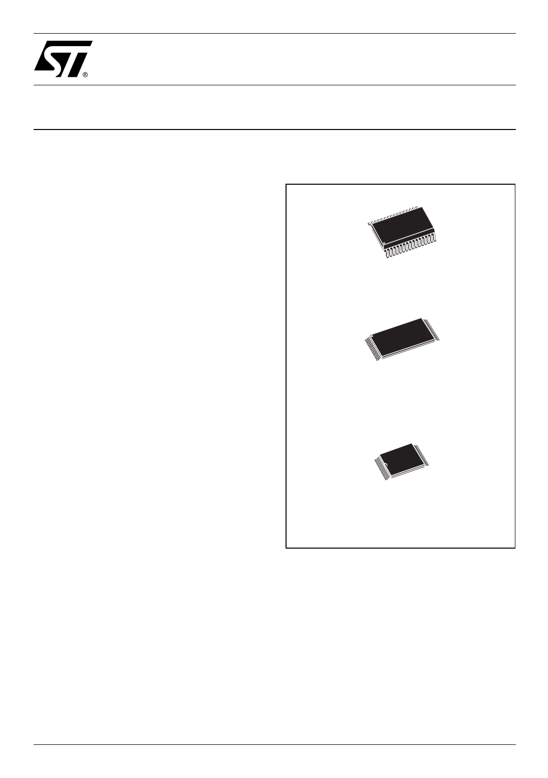
Figure 1. Packages
SO32 (MC)
TSOP32
8 x 20 mm
(N)
TSOP32
8 x 13.4 mm
(NK)
August 2003
1/20
1 page 
Figure 5. Block Diagram
A16
A7
DQ7
DQ0
E1 Ex
E2
W
M68AW127B
ROW
DECODER
MEMORY
ARRAY
I/O CIRCUITS
COLUMN
DECODER
A0 A6
G
AI05471
MAXIMUM RATING
Stressing the device above the rating listed in the
“Absolute Maximum Ratings” table may cause
permanent damage to the device. These are
stress ratings only and operation of the device at
these or any other conditions above those indicat-
ed in the Operating sections of this specification is
Table 2. Absolute Maximum Ratings
Symbol
Parameter
IO (1)
Output Current
TA Ambient Operating Temperature
TSTG
Storage Temperature
VCC Supply Voltage
VIO (2)
Input or Output Voltage
PD Power Dissipation
Note: 1. One output at a time, not to exceed 1 second duration.
2. Up to a maximum operating VCC of 3.6V only.
not implied. Exposure to Absolute Maximum Rat-
ing conditions for extended periods may affect de-
vice reliability. Refer also to the
STMicroelectronics SURE Program and other rel-
evant quality documents.
Value
20
–55 to 125
–65 to 150
–0.3 to 4.6
–0.5 to VCC +0.5
1
Unit
mA
°C
°C
V
V
W
5/20
5 Page 
M68AW127B
Write Mode
The M68AW127B is in the Write mode whenever
the W and E1 pins are Low and the E2 pin is High.
Either the Chip Enable input (E1) or the Write En-
able input (W) must be de-asserted during Ad-
dress transitions for subsequent write cycles.
Write begins with the concurrence of E1 being ac-
tive with W low. Therefore, address setup time is
referenced to Write Enable and Chip Enable as
tAVWL and tAVEH, respectively, and is determined
by the latter occurring edge.
The Write cycle can be terminated by the earlier
rising edge of E1, or W.
If the Output is enabled (E1 = Low, E2 = High and
G = Low), then W will return the outputs to high im-
pedance within tWLQZ of its falling edge. Care must
be taken to avoid bus contention in this type of op-
eration. Data input must be valid for tDVWH before
the rising edge of Write Enable, or for tDVEH before
the rising edge of E1, whichever occurs first, and
remain valid for tWHDX or tEHDX.
Figure 11. Write Enable Controlled, Write AC Waveforms
A0-A16
tAVEL
E1
E2
W
DQ0-DQ7
tAVAV
VALID
tAVWH
tELWH
tWHAX
tAVWL
tWLWH
tWLQZ
tWHDX
DATA INPUT
tDVWH
tWHQX
AI05478
11/20
11 Page | ||
| Páginas | Total 20 Páginas | |
| PDF Descargar | [ Datasheet M68AW127.PDF ] | |
Hoja de datos destacado
| Número de pieza | Descripción | Fabricantes |
| M68AW127 | 1Mbit 128K x8 / 3.0V Asynchronous SRAM | ST Microelectronics |
| M68AW127B | 1Mbit 128K x8 / 3.0V Asynchronous SRAM | ST Microelectronics |
| M68AW128M | 2 Mbit (128K x16) 3.0V Asynchronous SRAM | ST Microelectronics |
| Número de pieza | Descripción | Fabricantes |
| SLA6805M | High Voltage 3 phase Motor Driver IC. |
Sanken |
| SDC1742 | 12- and 14-Bit Hybrid Synchro / Resolver-to-Digital Converters. |
Analog Devices |
|
DataSheet.es es una pagina web que funciona como un repositorio de manuales o hoja de datos de muchos de los productos más populares, |
| DataSheet.es | 2020 | Privacy Policy | Contacto | Buscar |