|
|
|
PDF MC7815C Data sheet ( Hoja de datos )
| Número de pieza | MC7815C | |
| Descripción | THREE TERMINAL POSITIVE FIXED VOLTAGE REGULATORS | |
| Fabricantes | Motorola Semiconductors | |
| Logotipo | ||
Hay una vista previa y un enlace de descarga de MC7815C (archivo pdf) en la parte inferior de esta página. Total 16 Páginas | ||
|
No Preview Available !
Order this document by MC7800/D
Three-Terminal Positive
Voltage Regulators
These voltage regulators are monolithic integrated circuits designed as
fixed–voltage regulators for a wide variety of applications including local,
on–card regulation. These regulators employ internal current limiting,
thermal shutdown, and safe–area compensation. With adequate heatsinking
they can deliver output currents in excess of 1.0 A. Although designed
primarily as a fixed voltage regulator, these devices can be used with
external components to obtain adjustable voltages and currents.
• Output Current in Excess of 1.0 A
• No External Components Required
• Internal Thermal Overload Protection
• Internal Short Circuit Current Limiting
• Output Transistor Safe–Area Compensation
• Output Voltage Offered in 2% and 4% Tolerance
• Available in Surface Mount D2PAK and Standard 3–Lead Transistor
Packages
• Previous Commercial Temperature Range has been Extended to a
Junction Temperature Range of –40°C to +125°C
DEVICE TYPE/NOMINAL OUTPUT VOLTAGE
MC7805AC
LM340AT–5
MC7805C
5.0 V
MC7812C
LM340T–12
MC7815AC
12 V
LM340T–5
MC7806AC
MC7806C
6.0 V
LM340AT–15
MC7815C
LM340T–15
15 V
MC7808AC
MC7808C
8.0 V
MC7818AC
MC7818C
18 V
MC7809C
MC7812AC
LM340AT–12
9.0 V
12 V
MC7824AC
MC7824C
24 V
MC7800,
MC7800A, LM340,
LM340A Series
THREE–TERMINAL
POSITIVE FIXED
VOLTAGE REGULATORS
SEMICONDUCTOR
TECHNICAL DATA
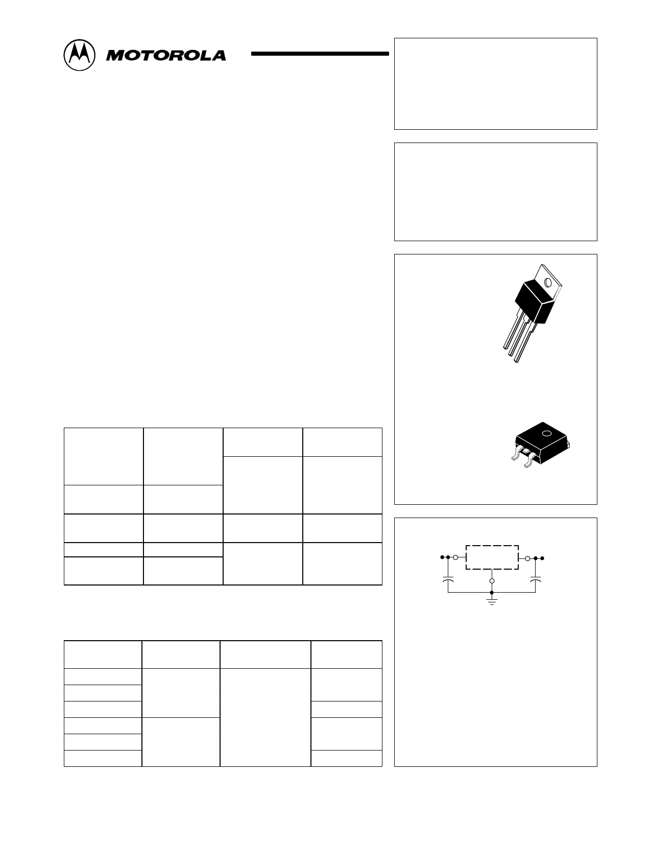
T SUFFIX
PLASTIC PACKAGE
CASE 221A
Heatsink surface
connected to Pin 2.
1
2
3
Pin 1. Input
2. Ground
3. Output
D2T SUFFIX
PLASTIC PACKAGE
CASE 936
(D2PAK)
12
3
Heatsink surface (shown as terminal 4 in
case outline drawing) is connected to Pin 2.
STANDARD APPLICATION
Input
Cin*
0.33 µF
MC78XX
Output
CO**
ORDERING INFORMATION
Device
Output Voltage
Operating
Tolerance
Temperature Range
Package
MC78XXACT
LM340AT–XX
2%
Insertion Mount
MC78XXACD2T
Surface Mount
MC78XXCT
TJ = –40° to +125°C
Insertion Mount
LM340T–XX
4%
MC78XXCD2T
Surface Mount
XX indicates nominal voltage.
MOTOROLA ANALOG IC DEVICE DATA
A common ground is required between the
input and the output voltages. The input voltage
must remain typically 2.0 V above the output
voltage even during the low point on the input
ripple voltage.
XX, These two digits of the type number
indicate nominal voltage.
* Cin is required if regulator is located an
appreciable distance from power supply
filter.
** CO is not needed for stability; however,
it does improve transient response. Values
of less than 0.1 µF could cause instability.
© Motorola, Inc. 1997
Rev 5
1
1 page 
MC7800, MC7800A, LM340, LM340A Series
ELECTRICAL CHARACTERISTICS (Vin = 11 V, IO = 1.0 A, TJ = Tlow to Thigh [Note 1], unless otherwise noted.)
MC7806AC
Characteristic
Symbol Min Typ Max
Output Voltage (TJ = 25°C)
Output Voltage (5.0 mA ≤ IO ≤ 1.0 A, PD ≤ 15 W)
8.6 Vdc ≤ Vin ≤ 21 Vdc
Line Regulation (Note 2)
8.6 Vdc ≤ Vin ≤ 25 Vdc, IO = 500 mA
9.0 Vdc ≤ Vin ≤ 13 Vdc, IO = 1.0 A
Load Regulation (Note 2)
5.0 mA ≤ IO ≤ 1.5 A, TJ = 25°C
5.0 mA ≤ IO ≤ 1.0 A
250 mA ≤ IO ≤ 750 mA
Quiescent Current
Quiescent Current Change
9.0 Vdc ≤ Vin ≤ 25 Vdc, IO = 500 mA
9.0 Vdc ≤ Vin ≤ 21 Vdc, IO = 1.0 A, TJ = 25°C
5.0 mA ≤ IO ≤ 1.0 A
Ripple Rejection
9.0 Vdc ≤ Vin ≤ 19 Vdc, f = 120 Hz, IO = 500 mA
Dropout Voltage (IO = 1.0 A, TJ = 25°C)
Output Noise Voltage (TA = 25°C)
10 Hz ≤ f ≤ 100 kHz
VO 5.88 6.0 6.12
VO 5.76 6.0 6.24
Regline
– 5.0 12
– 1.4 15
Regload
–
–
–
1.3 25
0.9 25
0.2 15
IB – 3.3 6.0
∆IB
– – 0.8
– – 0.8
– – 0.5
RR
58 65
–
VI – VO
–
2.0
–
Vn – 10 –
Output Resistance (f = 1.0 kHz)
Short Circuit Current Limit (TA = 25°C)
Vin = 35 Vdc
Peak Output Current (TJ = 25°C)
Average Temperature Coefficient of Output Voltage
rO
ISC
Imax
TCVO
– 0.9 –
– 0.2 –
– 2.2 –
– –0.3 –
Unit
Vdc
Vdc
mV
mV
mA
mA
dB
Vdc
µV/VO
mΩ
A
A
mV/°C
ELECTRICAL CHARACTERISTICS (Vin = 14 V, IO = 500 mA, TJ = Tlow to Thigh [Note 1], unless otherwise noted.)
MC7808C
Characteristic
Symbol Min Typ Max Unit
Output Voltage (TJ = 25°C)
Output Voltage (5.0 mA ≤ IO ≤ 1.0 A, PD ≤ 15 W)
10.5 Vdc ≤ Vin ≤ 23 Vdc
Line Regulation, TJ = 25°C, (Note 2)
10.5 Vdc ≤ Vin ≤ 25 Vdc
11 Vdc ≤ Vin ≤ 17 Vdc
Load Regulation, TJ = 25°C (Note 2)
5.0 mA ≤ IO ≤ 1.5 A
Quiescent Current
Quiescent Current Change
10.5 Vdc ≤ Vin ≤ 25 Vdc
5.0 mA ≤ IO ≤ 1.0 A
Ripple Rejection
11.5 Vdc ≤ Vin ≤ 18 Vdc, f = 120 Hz
Dropout Voltage (IO = 1.0 A, TJ = 25°C)
Output Noise Voltage (TA = 25°C)
10 Hz ≤ f ≤ 100 kHz
VO 7.7 8.0 8.3 Vdc
VO 7.6 8.0 8.4 Vdc
Regline
Regload
–
–
–
mV
6.0 32
1.7 16
1.4 35 mV
IB – 3.3 8.0 mA
∆IB mA
– – 1.0
– – 0.5
RR
56 62
– dB
VI – VO
–
2.0
– Vdc
Vn – 10 – µV/VO
NOTES: 1. Tlow = –40°C for MC78XXAC, C Thigh = +125°C for MC78XXAC, C
2. Load and line regulation are specified at constant junction temperature. Changes in VO due to heating effects must be taken into account
separately. Pulse testing with low duty cycle is used.
MOTOROLA ANALOG IC DEVICE DATA
5
5 Page 
MC7800, MC7800A, LM340, LM340A Series
ELECTRICAL CHARACTERISTICS (Vin = 27 V, IO = 1.0 A, TJ = Tlow to Thigh [Note 1], unless otherwise noted.)
MC7818AC
Characteristic
Symbol Min Typ Max
Output Voltage (TJ = 25°C)
Output Voltage (5.0 mA ≤ IO ≤ 1.0 A, PD ≤ 15 W)
21 Vdc ≤ Vin ≤ 33 Vdc
Line Regulation (Note 2)
21 Vdc ≤ Vin ≤ 33 Vdc, IO = 500 mA
24 Vdc ≤ Vin ≤ 30 Vdc, IO = 1.0 A
24 Vdc ≤ Vin ≤ 30 Vdc, IO = 1.0 A, TJ = 25°C
20.6 Vdc ≤ Vin ≤ 33 Vdc, IO = 1.0 A, TJ = 25°C
Load Regulation (Note 2)
5.0 mA ≤ IO ≤ 1.5 A, TJ = 25°C
5.0 mA ≤ IO ≤ 1.0 A
250 mA ≤ IO ≤ 750 mA
Quiescent Current
Quiescent Current Change
21 Vdc ≤ Vin ≤ 33 Vdc, IO = 500 mA
21.5 Vdc ≤ Vin ≤ 30 Vdc, TJ = 25°C
5.0 mA ≤ IO ≤ 1.0 A
Ripple Rejection
22 Vdc ≤ Vin ≤ 32 Vdc, f = 120 Hz, IO = 500 mA
Dropout Voltage (IO = 1.0 A, TJ = 25°C)
Output Noise Voltage (TA = 25°C)
10 Hz ≤ f ≤ 100 kHz
VO 17.64 18 18.36
VO 17.3 18 18.7
Regline
Regload
IB
∆IB
RR
–
–
–
–
–
–
–
–
–
–
–
53
9.5 22
3.2 25
3.2 10.5
8.0 22
2.0 25
1.8 25
1.5 15
3.5 6.0
– 0.8
– 0.8
– 0.5
57 –
VI – VO
–
2.0
–
Vn – 10 –
Output Resistance f = 1.0 kHz
Short Circuit Current Limit (TA = 25°C)
Vin = 35 Vdc
Peak Output Current (TJ = 25°C)
Average Temperature Coefficient of Output Voltage
rO
ISC
Imax
TCVO
– 1.3 –
– 0.2 –
– 2.2 –
– –1.5 –
Unit
Vdc
Vdc
mV
mV
mA
mA
dB
Vdc
µV/VO
mΩ
A
A
mV/°C
ELECTRICAL CHARACTERISTICS (Vin = 33 V, IO = 500 mA, TJ = Tlow to Thigh [Note 1], unless otherwise noted.)
MC7824C
Characteristic
Symbol Min Typ Max
Output Voltage (TJ = 25°C)
VO 23 24 25
Output Voltage (5.0 mA ≤ IO ≤ 1.0 A, PD ≤ 15 W)
27 Vdc ≤ Vin ≤ 38 Vdc
VO 22.8 24 25.2
Line Regulation, (Note 2)
27 Vdc ≤ Vin ≤ 38 Vdc
30 Vdc ≤ Vin ≤ 36 Vdc
Regline
– 2.7 60
– 2.7 48
Load Regulation, (Note 2)
5.0 mA ≤ IO ≤ 1.5 A
Regload
–
4.4 65
Quiescent Current
IB – 3.6 6.5
Quiescent Current Change
27 Vdc ≤ Vin ≤ 38 Vdc
5.0 mA ≤ IO ≤ 1.0 A
∆IB
– – 1.0
– – 0.5
NOTES: 1. Tlow = –40°C for MC78XXAC, C Thigh = +125°C for MC78XXAC, C
2. Load and line regulation are specified at constant junction temperature. Changes in VO due to heating effects must be taken into account
separately. Pulse testing with low duty cycle is used.
Unit
Vdc
Vdc
mV
mV
mA
mA
MOTOROLA ANALOG IC DEVICE DATA
11
11 Page | ||
| Páginas | Total 16 Páginas | |
| PDF Descargar | [ Datasheet MC7815C.PDF ] | |
Hoja de datos destacado
| Número de pieza | Descripción | Fabricantes |
| MC7815 | 3-Terminal 1A Positive Voltage Regulator | Fairchild |
| MC7815 | (MC7800 Series) Three Terminal Positive Fixed Voltage Regulators | Motorola Semiconductor |
| MC7815A | 3-Terminal 1A Positive Voltage Regulator | Fairchild |
| MC7815AC | THREE TERMINAL POSITIVE FIXED VOLTAGE REGULATORS | Motorola Semiconductors |
| Número de pieza | Descripción | Fabricantes |
| SLA6805M | High Voltage 3 phase Motor Driver IC. |
Sanken |
| SDC1742 | 12- and 14-Bit Hybrid Synchro / Resolver-to-Digital Converters. |
Analog Devices |
|
DataSheet.es es una pagina web que funciona como un repositorio de manuales o hoja de datos de muchos de los productos más populares, |
| DataSheet.es | 2020 | Privacy Policy | Contacto | Buscar |