|
|
|
PDF M39432-10VNC6T Data sheet ( Hoja de datos )
| Número de pieza | M39432-10VNC6T | |
| Descripción | Single Chip 4 Mbit Flash Memory and 256 Kbit Parallel EEPROM | |
| Fabricantes | ST Microelectronics | |
| Logotipo | ||
Hay una vista previa y un enlace de descarga de M39432-10VNC6T (archivo pdf) en la parte inferior de esta página. Total 28 Páginas | ||
|
No Preview Available !
M39432
Single Chip 4 Mbit Flash Memory and
256 Kbit Parallel EEPROM
s Multiple Memories on a Single Chip:
– 4 Mbit Flash Memory (organised as 8 sectors)
– 256 Kbit EEPROM
– 64 Byte One Time Programmable Memory
s CONCURRENT Mode (Read Flash while
writing to EEPROM)
s WRITE, PROGRAM and ERASE Status Bits
s 2.7V to 3.6V Single Supply Voltage for
PROGRAM, ERASE and READ Operations
s 100 ns Access Time (Flash and EEPROM
blocks)
s Low Power Consumption
– 60 µA Stand-by mode (maximum)
– Deep Power Down mode:
6 µA (maximum), 200 nA (typical)
s Standard Flash Memory Package
s 100,000 Erase/Write Cycles (minimum)
s 10 Year Data Retention (minimum)
DESCRIPTION
The M39432 is a single supply voltage memory
device combining Flash memory and EEPROM on
a single chip. The memory is mapped in two
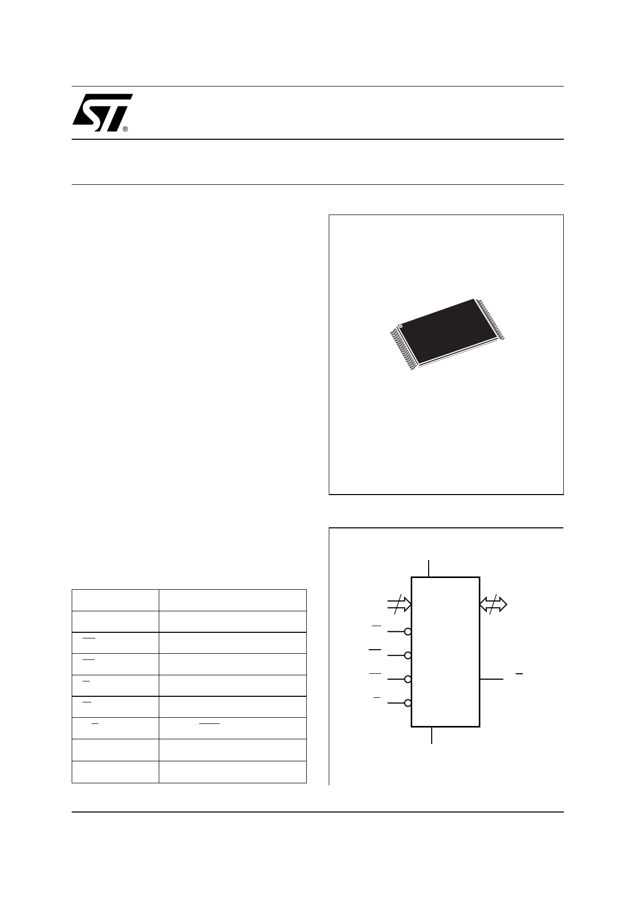
Table 1. Signal Names
A0-A18
Address Inputs
DQ0-DQ7
Data Inputs / Outputs
EE EEPROM Block Enable
EF Flash Block Enable
G Output Enable
W Write Enable
R/B Ready/Busy Output
VCC Supply Voltage
VSS Ground
TSOP40 (NC)
10 x 20 mm
Figure 1. Logic Diagram
VCC
19
A0-A18
W
EE
EF
G
M39432
8
DQ0-DQ7
R/B
VSS
AI01946
November 1999
1/28
1 page 
M39432
Table 4. Instructions 1
Instruction EE EF Cycle 1
Cycle 2
Cycle 3
Cycle 4
Cycle 5 Cycle 6 Cycle 7
Read
Manufacturer
Identifier 2
1
0
AAh 55h
@5555h @2AAAh
90h
@5555h
Read Identifier
with (A0,A1,A6)
set to (0,0,0)
Read Flash
Identifier 2
1
0
AAh 55h
@5555h @2AAAh
90h
@5555h
Read Identifier
with (A0,A1,A6)
set to (1,0,0)
Read OTP Row
0
1
AAh 55h 90h
@5555h @2AAAh @5555h
Read
Byte 1
Read
Byte 2
Read
Byte N
Read Sector
Protection Status2 1
0
AAh 55h 90h
@5555h @2AAAh @5555h
Read Identifier
with (A0,A1,A6)
set to (0,1,0)
Program a Byte of
Flash Memory
1
0
AAh 55h A0h
@5555h @2AAAh @5555h
Data
@ Address
Erase a Sector of
Flash Memory
1
0
AAh 55h 80h
@5555h @2AAAh @5555h
AAh
@5555h
55h
@2AAAh
30h
@ Sector
address
30h
@ Sector
address3
Erase the Whole
of Flash Memory
1
0
AAh 55h 80h
@5555h @2AAAh @5555h
AAh
@5555h
55h 10h
@2AAAh @5555h
Suspend Sector
Erase
B0h
1 0 @any
address
Resume Sector
Erase
30h
1 0 @any
address
EEPROM Power
Down
0
1
AAh 55h 30h
@5555h @2AAAh @5555h
Deep Power
Down
1
0
20h
@5555h
SDP Enable
(EEPROM)
0
1
AAh 55h A0h
@5555h @2AAAh @5555h
Write
Byte 1
Write
Byte 2
Write
Byte N
SDP Disable
(EEPROM)
0
1
AAh 55h 80h
@5555h @2AAAh @5555h
AAh
@5555h
55h 20h
@2AAAh @5555h
Write OTP Row
0
1
AAh 55h B0h
@5555h @2AAAh @5555h
Write
Byte 1
Write
Byte 2
Write
Byte N
Return (from OTP
Read or
EEPROM Power
Down)
0
1
F0h
@any
address
Reset
1
0
AAh
@5555h
55h
@2AAAh
F0h
@any
address
Reset (short
instruction)
F0h
1 0 @any
address
Note: 1. AAh @ 5555h means “Write the value AAh at the address 5555h”.
2. This instruction can also be performed as a Verify operation with A9=VID (please see the section entitled “Flash Sector Protection
and Unprotection” on page 18).
3. Addresses of additional sectors to be erased must be entered within a time-out of 80 µs of each other.
5/28
5 Page 
M39432
All bytes must be located on the same page
address (A6-A18 must be the same for all bytes).
Otherwise, the Page Write operation is not
executed.
As with the single byte Write operation, described
above, the DQ6 and DQ7 lines can be used to
detect the beginning and end of the internally
controlled phase of the Page Write cycle.
EEPROM Block Software Data Protection
The Software Data Protection (SDP) instruction
protects the EEPROM block from inadvertent
Write operations, for example that might be
caused under uncontrolled bus conditions.
By default, the M39432 is shipped in the
unprotected state: the EEPROM memory can be
written to normally. After the SDP Enable
instruction, the device enters the Protected Mode,
and further write operations have no effect on the
EEPROM contents.
The device remains in this mode until a valid SDP
Disable instruction has been received. The device
then returns to its unprotected state.
To enable the Software Data Protection, the
device has to be written (under Page Write timing
conditions) with three specific data bytes at three
specific memory locations (each location on a
different page) as shown in Table 4 and Figure 6.
Figure 6 shows that there are three ways to use
the SDP-Enable instruction. Firstly, as shown in
the flow-chart on the left, it can be used as a three-
byte instruction that sets the SDP. Secondly, it can
be used as a way of writing data to the EEPROM
even when the SDP is set. Only if the data to be
written is preceeded by the correct three byte
instruction, and all the bytes are written with the
correct Page Write timing, will the request be
accepted, and acted on. Lastly, if the SDP is
currently not set, the instruction can be used as a
means of performing a Page Write, and setting the
SDP at the same time.
To disable the Software Data Protection the user
has to write specific data bytes into six different
locations (under Page Write timing conditions)
with different bytes being written on different
pages, as shown in Figure 7.
The Software Data Protection state is held
internally in a non-volatile latch (and so the state is
remembered across power-on and power-off
events. Access to this latch, through the SDP
Enable and Disable instructions, require the same
write time (tWC) as for the non-volatile memory.
This Write operation can be monitored on the
Toggle bit (status bit DQ6) and the Ready/Busy
pin, but not on DQ7. The Ready/Busy output is
driven low from the first written byte (the first Write
AAh,@5555h of the SDP sequence) until the
completion of the internal Page Write sequence.
Writing the OTP Row
Writing in the OTP row is enabled by an instruction
composed of three specific Write operations,
under Page Write timing conditions, as shown in
Table 4. These instructions write data bytes at
three specific memory locations, each location on
a different page, followed by the data (between 1
and 64 bytes) that is to be stored in the OTP row.
This action can only be performed once. Even by
writing fewer than all 64 bytes on the first write to
the OTP row, none of the bytes, including any that
have not yet been changed, can be modified at a
later time.
When accessing the OTP row, the only least
significant address bits (A0 to A6) are decoded. Of
these, A6 must be held at 0.
Writing the EEPROM Block Identifier
The EEPROM Block Identifier (64 bytes) can be
written with a single Write operation with VID
applied on A9, and A6 is driven low, as shown in
Table 8.
Programming the Flash Block
Programming a byte in the Flash memory block is
performed using the instruction shown in Table 4.
This is different to writing data to the EEPROM
block, which is performed as an operation (as
shown in Table 3). Similarly, an instruction is
needed when erasing a sector of Flash memory.
The Program instruction is a sequence of three
specific Write operations, followed by a Write
operation bearing the address and data that is to
be written (as shown in Table 4). The M39432
automatically starts and performs the
programming after the fourth write operation. In
this way, the Flash memory block can be
programmed a byte at a time.
The Flash memory block rejects any further
instructions that arrive during the execution of the
Program instruction. During programming, the
memory status may be checked by reading the
status bits DQ7, DQ6 and DQ5, as described on
page 8.
Data Polling using DQ7. Please see the
description on page 8.
Data Toggling using DQ6. Please see the
description on page 8.
Flash Block Erase
A Write to the EEPROM block is an operation that
triggers an automatic, internal sequence of Byte
Erase followed by Byte Write.
The Flash memory block, though, is different.
Writing to the Flash memory block first requires an
explicit Erase operation.
The Flash memory Erase instruction cannot be
addressed to a byte at a time. The Erase can only
11/28
11 Page | ||
| Páginas | Total 28 Páginas | |
| PDF Descargar | [ Datasheet M39432-10VNC6T.PDF ] | |
Hoja de datos destacado
| Número de pieza | Descripción | Fabricantes |
| M39432-10VNC6T | Single Chip 4 Mbit Flash Memory and 256 Kbit Parallel EEPROM | ST Microelectronics |
| Número de pieza | Descripción | Fabricantes |
| SLA6805M | High Voltage 3 phase Motor Driver IC. |
Sanken |
| SDC1742 | 12- and 14-Bit Hybrid Synchro / Resolver-to-Digital Converters. |
Analog Devices |
|
DataSheet.es es una pagina web que funciona como un repositorio de manuales o hoja de datos de muchos de los productos más populares, |
| DataSheet.es | 2020 | Privacy Policy | Contacto | Buscar |