|
|
|
PDF IDT5V2528APGI Data sheet ( Hoja de datos )
| Número de pieza | IDT5V2528APGI | |
| Descripción | 2.5V / 3.3V PHASE-LOCK LOOP CLOCK DRIVER ZERO DELAY BUFFER | |
| Fabricantes | Integrated Device | |
| Logotipo | ||
Hay una vista previa y un enlace de descarga de IDT5V2528APGI (archivo pdf) en la parte inferior de esta página. Total 7 Páginas | ||
|
No Preview Available !
IDT5V2528/A
2.5 / 3.3V PHASE-LOCK LOOP CLOCK DRIVER
2.5V / 3.3V PHASE-LOCK
LOOP CLOCK DRIVER
ZERO DELAY BUFFER
INDUSTRIALTEMPERATURERANGE
IDT5V2528/A
FEATURES:
• Operates at 3.3V VDD/AVDD and 2.5V/3.3V VDDQ
• 1:10 fanout
• 3-level inputs for output control
• External feedback (FBIN) pin is used to synchronize the
outputs to the clock input signal
• No external RC network required for PLL loop stability
• Configurable 2.5V or 3.3V LVTTL outputs
• tPD Phase Error at 100MHz to 166MHz: ±150ps
• Jitter (peak-to-peak) at 133MHz and 166MHz: ±75ps
• Spread spectrum compatible
• Operating Frequency:
− Std: 25MHz to 140MHz
− A: 25MHz to 167MHz
• Available in TSSOP package
DESCRIPTION:
The IDT5V2528 is a high performance, low-skew, low-jitter, phase-lock
loop (PLL) clock driver. It uses a PLL to precisely align, in both frequency
and phase, the feedback (FBOUT) output to the clock (CLK) input signal.
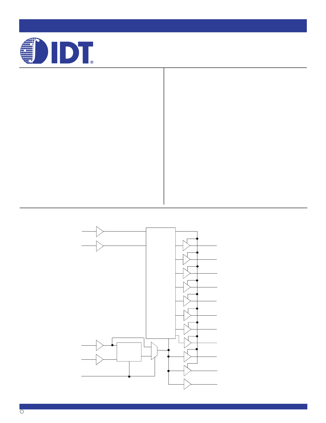
FUNCTIONAL BLOCK DIAGRAM
The IDT5V2528 inputs, PLL core, Y0, Y1, and FBOUT buffers operate from
the 3.3V VDD and AVDD power supply pins.
One bank of ten outputs provide low-skew, low-jitter copies of CLK. Of
the ten outputs, up to seven may be configured for 2.5V or 3.3V LVTTL
outputs. The number of 2.5V outputs is controlled by 3-level input signals
G_Ctrl and T_Ctrl, and by connecting the appropriate VDDQ pins to 2.5V or
3.3V. The 3-level input signals may be hard-wired to high-mid-low levels.
Output signal duty cycles are adjusted to 50 percent, independent of the duty
cycle at CLK. The outputs can be enabled or disabled via the G_Ctrl input.
When the G_Ctrl input is mid or high, the outputs switch in phase and
frequency with CLK; when the G_Ctrl is low, all outputs (except FBOUT) are
disabled to the logic-low state.
Unlike many products containing PLLs, the IDT5V2528 does not require
external RC networks. The loop filter for the PLL is included on-chip,
minimizing component count, board space, and cost.
Because it is based on PLL circuitry, the IDT5V2528 requires a
stabilization time to achieve phase lock of the feedback signal to the
reference signal. This stabilization time is required, following power up and
application of a fixed-frequency, fixed-phase signal at CLK, as well as
following any changes to the PLL reference or feedback signals. The PLL
can be bypassed for test purposes by strapping AVDD to ground.
28
G_Ctrl
T_Ctrl 1
MODE
SELECT
CLK 6
7
FBIN
AVDD
5
PLL
The IDT logo is a registered trademark of Integrated Device Technology, Inc.
INDUSTRIAL TEMPERATURE RANGE
c 2002 Integrated Device Technology, Inc.
1
3
TY0, VDDQ pin 4
26
TY1, VDDQ pin 25
24
TY2, VDDQ pin 25
17
TY3, VDDQ pin 15
16
TY4, VDDQ pin 15
13
TY5, VDDQ pin 11
12
TY6, VDDQ pin 11
10
TY7, VDDQ pin 11
20
Y0, VDD pin 21
19
Y1, VDD pin 21
22
FBOUT, VDD pin 21
JUNE 2003
DSC 5971/11
1 page 
IDT5V2528/A
2.5 / 3.3V PHASE-LOCK LOOP CLOCK DRIVER
INDUSTRIALTEMPERATURERANGE
INPUT TIMING REQUIREMENTS OVER OPERATING RANGE
5V2528
5V2528A
Min
Max Min
Max
fCLOCK
Clock frequency
25
140 25
167
Input clock duty cycle
40% 60% 40% 60%
tLOCK Stabilizationtime(1)
11
Units
MHz
ms
NOTE:
1.Time required for the integrated PLL circuit to obtain phase lock of its feedback signal to its reference signal. For phase lock to be obtained, a fixed-frequency, fixed-phase reference
signal must be present at CLK. Until phase lock is obtained, the specifications for propagation delay, skew, and jitter parameters given in the switching characteristics table are
not applicable.
SWITCHING CHARACTERISTICS OVER OPERATING RANGE - 5V2528(1)
Symbol
tPHASE error
tPHASE error - jitter(3)
tSK1(0)(4)
tSK2(0)(4)
tSK3(0)(4,5)
tJ
tR
tF
tR
tF
Parameter(2)
Phase Error from Rising Edge CLK to Rising Edge FBIN (100MHz-133MHz)
Phase Error minus Jitter from Rising Edge CLK to Rising Edge FBIN (133MHz)
Output Skew between 3.3V Outputs
Output Skew between 2.5V Outputs
Output Skew between 2.5V and 3.3V Outputs
Cycle-to-Cycle Output Jitter (Peak-to-Peak) at 133MHz
Duty Cycle
Output Rise Time for 3.3V Outputs (20% to 80%)
Output Fall Time for 3.3V Outputs (20% to 80%)
Output Rise Time for 2.5V Outputs (20% to 80%)
Output Fall Time for 2.5V Outputs (20% to 80%)
Min.
–150
–50
—
—
—
–75
45
0.8
0.8
0.5
0.5
Typ. Max.
— 150
— 50
— 150
— 150
— 200
— 75
— 55
— 2.1
— 2.1
— 1.5
— 1.5
Unit
ps
ps
ps
ps
ps
ps
%
ns
ns
ns
ns
SWITCHING CHARACTERISTICS OVER OPERATING RANGE - 5V2528A(1)
Symbol
tPHASE error
tPHASE error - jitter(3)
tSK1(0)(4)
tSK2(0)(4)
tSK3(0)(4,5)
tJ
tR
tF
tR
tF
Parameter(2)
Phase Error from Rising Edge CLK to Rising Edge FBIN (100MHz-166MHz)
Phase Error minus Jitter from Rising Edge CLK to Rising Edge FBIN (166MHz)
Output Skew between 3.3V Outputs
Output Skew between 2.5V Outputs
Output Skew between 2.5V and 3.3V Outputs 25MHz to 133MHz
133MHz to 166MHz
Cycle-to-Cycle Output Jitter (Peak-to-Peak) at 166MHz
Duty Cycle
Output Rise Time for 3.3V Outputs (20% to 80%)
Output Fall Time for 3.3V Outputs (20% to 80%)
Output Rise Time for 2.5V Outputs (20% to 80%)
Output Fall Time for 2.5V Outputs (20% to 80%)
Min.
–150
–50
—
—
—
—
–75
45
0.8
0.8
0.5
0.5
Typ. Max.
— 150
— 50
— 150
— 150
— 200
— 250
— 75
— 55
— 2.1
— 2.1
— 1.5
— 1.5
NOTES:
1. All parameters are measured with the following load conditions: 30pF || 500Ω for 3.3V outputs and 20pF || 500Ω for 2.5V outputs.
2. The specifications for parameters in this table are applicable only after any appropriate stabilization time has elapsed.
3. Phase error does not include jitter.
4. All skew parameters are only valid for equal loading of all outputs.
5. Measured for VDDQ = 2.3V and 3V, 2.5V and 3.3V, or 2.7V and 3.6V.
Unit
ps
ps
ps
ps
ps
ps
%
ns
ns
ns
ns
5
5 Page | ||
| Páginas | Total 7 Páginas | |
| PDF Descargar | [ Datasheet IDT5V2528APGI.PDF ] | |
Hoja de datos destacado
| Número de pieza | Descripción | Fabricantes |
| IDT5V2528APG | 2.5V / 3.3V PHASE-LOCK LOOP CLOCK DRIVER ZERO DELAY BUFFER | Integrated Device |
| IDT5V2528APGG | 2.5V / 3.3V PHASE-LOCK LOOP CLOCK DRIVER ZERO DELAY BUFFER | Integrated Device |
| IDT5V2528APGGI | 2.5V / 3.3V PHASE-LOCK LOOP CLOCK DRIVER ZERO DELAY BUFFER | Integrated Device |
| IDT5V2528APGI | 2.5V / 3.3V PHASE-LOCK LOOP CLOCK DRIVER ZERO DELAY BUFFER | Integrated Device |
| Número de pieza | Descripción | Fabricantes |
| SLA6805M | High Voltage 3 phase Motor Driver IC. |
Sanken |
| SDC1742 | 12- and 14-Bit Hybrid Synchro / Resolver-to-Digital Converters. |
Analog Devices |
|
DataSheet.es es una pagina web que funciona como un repositorio de manuales o hoja de datos de muchos de los productos más populares, |
| DataSheet.es | 2020 | Privacy Policy | Contacto | Buscar |