|
|
|
PDF IDT2308-3DCI Data sheet ( Hoja de datos )
| Número de pieza | IDT2308-3DCI | |
| Descripción | 3.3V ZERO DELAY CLOCK MULTIPLIER | |
| Fabricantes | Integrated Device | |
| Logotipo | ||
Hay una vista previa y un enlace de descarga de IDT2308-3DCI (archivo pdf) en la parte inferior de esta página. Total 13 Páginas | ||
|
No Preview Available !
www.DataSheet4U.com
IDT2308
3.3V ZERO DELAY CLOCK MULTIPLIER
COMMERCIAL AND INDUSTRIAL TEMPERATURE RANGES
3.3V ZERO DELAY
CLOCK MULTIPLIER
IDT2308
FEATURES:
• Phase-Lock Loop Clock Distribution for Applications ranging
from 10MHz to 133MHz operating frequency
• Distributes one clock input to two banks of four outputs
• Separate output enable for each output bank
• External feedback (FBK) pin is used to synchronize the outputs
to the clock input
• Output Skew <200 ps
• Low jitter <200 ps cycle-to-cycle
• 1x, 2x, 4x output options (see table):
– IDT2308-1 1x
– IDT2308-2 1x, 2x
– IDT2308-3 2x, 4x
– IDT2308-4 2x
– IDT2308-1H, -2H, and -5H for High Drive
• No external RC network required
• Operates at 3.3V VDD
• Available in SOIC and TSSOP packages
DESCRIPTION:
The IDT2308 is a high-speed phase-lock loop (PLL) clock multiplier. It is
designed to address high-speed clock distribution and multiplication applica-
tions. The zero delay is achieved by aligning the phase between the incoming
clock and the output clock, operable within the range of 10 to 133MHz.
The IDT2308 has two banks of four outputs each that are controlled via two
select addresses. By proper selection of input addresses, both banks can be
put in tri-state mode. In test mode, the PLL is turned off, and the input clock
directly drives the outputs for system testing purposes. In the absence of an
input clock, the IDT2308 enters power down, and the outputs are tri-stated. In
this mode, the device will draw less than 25µA.
The IDT2308 is available in six unique configurations for both pre-
scaling and multiplication of the Input REF Clock. (See available options
table.)
The PLL is closed externally to provide more flexibility by allowing the user
to control the delay between the input clock and the outputs.
The IDT2308 is characterized for both Industrial and Commercial operation.
NOTE: For new designs, refer to AN-233.
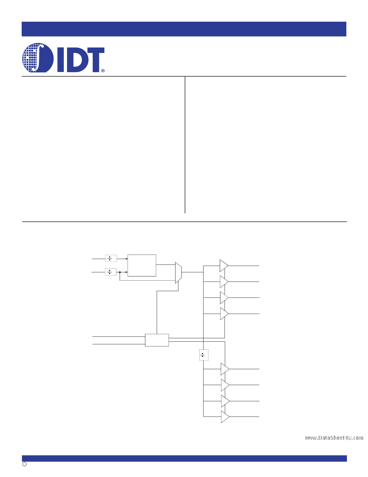
FUNCTIONAL BLOCK DIAGRAM
(-3, -4)
16
FBK
2
1
REF
2
(-5)
PLL
2
CLKA1
3
CLKA2
14
CLKA3
15
CLKA4
S2 8
S1 9
Control
Logic
(-2, -3) 2
6
CLKB1
7
CLKB2
10
CLKB3
11
CLKB4
The IDT logo is a registered trademark of Integrated Device Technology, Inc.
COMMERCIAL AND INDUSTRIAL
c 2003 Integrated Device Technology, Inc.
DataSheet4 U .com
TEMPERATURE
1
RANGES
APRIL 2003
DSC 5173/9
1 page 
www.DataSheet4U.com
IDT2308
3.3V ZERO DELAY CLOCK MULTIPLIER
COMMERCIAL AND INDUSTRIAL TEMPERATURE RANGES
OPERATING CONDITIONS- COMMERCIAL
Symbol
Parameter
Test Conditions
VDD Supply Voltage
TA OperatingTemperature(AmbientTemperature)
CL Load Capacitance below 100MHz
Load Capacitance from 100MHz to 133MHz
CIN InputCapacitance(1)
NOTE:
1. Applies to both REF and FBK.
Min. Max. Unit
3 3.6 V
0 70 °C
— 30 pF
— 15 pF
— 7 pF
DC ELECTRICAL CHARACTERISTICS - COMMERCIAL
Symbol
Parameter
Conditions
VIL Input LOW Voltage Level
VIH Input HIGH Voltage Level
IIL Input LOW Current
VIN = 0V
IIH Input HIGH Current
VIN = VDD
VOL OutputLOWVoltage
IOL = 8mA (-1, -2, -3, -4)
IOL = 12mA (-1H, -2H, -5H)
VOH Output HIGH Voltage
IOH = -8mA (-1, -2, -3, -4)
IOH = -12mA (-1H, -2H, -5H)
IDD_PD
Power Down Current
REF = 0MHz (S2 = S1 = H)
100MHz CLKA (-1, -2, -3, -4)
100MHz CLKA (-1H, -2H, -5H)
IDD Supply Current
Unloaded Outputs
66MHz CLKA (-1, -2, -3, -4)
Select Inputs at VDD or GND 66MHz CLKA (-1H, -2H, -5H)
33MHz CLKA (-1, -2, -3, -4)
33MHz CLKA (-1H, -2H, -5H)
Min.
—
2
—
—
—
2.4
—
—
—
—
—
—
—
Typ.(1)
—
—
—
—
—
Max.
0.8
—
50
100
0.4
——
— 12
— 45
— 70
— 32
— 50
— 18
— 30
Unit
V
V
µA
µA
V
V
µA
mA
DataSheet4 U .com
5
5 Page 
www.DataSheet4U.com
IDT2308
3.3V ZERO DELAY CLOCK MULTIPLIER
COMMERCIAL AND INDUSTRIAL TEMPERATURE RANGES
TYPICAL DUTY CYCLE(1) AND IDD TRENDS(2) FOR IDT2308-1H, -2H, AND -5H
Duty Cycle vs VDD
(for 30pf loads over frequency - 3.3V, 25C)
60
58
56
54
52
50
48
46
44
42
40
3
60
58
56
3.1 3.2 3.3 3.4 3.5
VDD (V)
Duty Cycle vs Frequency
(for 30pf loads over temperature - 3.3V)
54
52
50
48
46
44
42
40
20
40
60 80 100 120
Frequency (MHz)
IDD vs Number of Loaded Outputs
(for 30pf loads over frequency - 3.3V, 25C)
160
140
120
3.6
140
100
80
60
33MHz
66MHz
100MHz
-40C
0C
25C
70C
85C
33MHz
66MHz
100MHz
60
58
56
54
52
50
48
46
44
42
40
3
60
58
56
54
52
50
48
46
44
42
40
20
160
140
120
Duty Cycle vs VDD
(for 15pF loads over frequency - 3.3V, 25C)
3.1 3.2 3.3 3.4 3.5
VDD (V)
Duty Cycle vs Frequency
(for 15pF loads over temperature - 3.3V)
3.6
40 60 80 100 120 140
Frequency (MHz)
IDD vs Number of Loaded Outputs
(for 15pF loads over frequency - 3.3V, 25C)
100
80
60
33MHz
66MHz
100MHz
133MHz
-40C
0C
25C
70C
85C
33MHz
66MHz
100MHz
40 40
20 20
0
0
2 46 8
0
0
2 46 8
NOTES:
Number of Loaded Outputs
Number of Loaded Outputs
1. Duty Cycle is taken from typical chip measured at 1.4V.
2. IDD data is calculated from IDD = ICORE + nCVf, where ICORE is the Unloaded Current (n = Number of Outputs; C = Capacitance Load per Output (F); V = Voltage Supply(V);
f = Frequency (Hz).
11
DataSheet4 U .com
11 Page | ||
| Páginas | Total 13 Páginas | |
| PDF Descargar | [ Datasheet IDT2308-3DCI.PDF ] | |
Hoja de datos destacado
| Número de pieza | Descripción | Fabricantes |
| IDT2308-3DC | 3.3V ZERO DELAY CLOCK MULTIPLIER | Integrated Device |
| IDT2308-3DCI | 3.3V ZERO DELAY CLOCK MULTIPLIER | Integrated Device |
| Número de pieza | Descripción | Fabricantes |
| SLA6805M | High Voltage 3 phase Motor Driver IC. |
Sanken |
| SDC1742 | 12- and 14-Bit Hybrid Synchro / Resolver-to-Digital Converters. |
Analog Devices |
|
DataSheet.es es una pagina web que funciona como un repositorio de manuales o hoja de datos de muchos de los productos más populares, |
| DataSheet.es | 2020 | Privacy Policy | Contacto | Buscar |