|
|
|
PDF M66222SP Data sheet ( Hoja de datos )
| Número de pieza | M66222SP | |
| Descripción | 128 x 8-BIT x 2 MAIL-BOX | |
| Fabricantes | Mitsubishi | |
| Logotipo | ||
Hay una vista previa y un enlace de descarga de M66222SP (archivo pdf) en la parte inferior de esta página. Total 8 Páginas | ||
|
No Preview Available !
MITMSIUTBSUISBHIIS〈HDIIG〈DITIGAILTAALSSAPS〉SP〉
M6622M26S62P22/SFPP/FP
DESCRIPTION
The M66222 is a mail box that incorporates two complete CMOS
shared memory cells of 128 × 8-bit configuration using high-
performance silicon gate CMOS process technology, and are
equipped with two access ports of A and B.
Access ports A and B are equipped with independent addresses CS,
WE and OE control pins and I/O pins to allow independent and
asynchronous read/write operations individually. This product
exclusively performs a write operation from A port and a read operation
from B port for one memory, and a read operation from A port and a
write operation from B port for the other memory.
FEATURES
• Memory configuration of 128 × 8 bits × 2 memory areas
• High-speed access, address access time 40ns (typ.)
• Complete asynchronous accessibility from ports A and B
• Fixed read/write access ports for memory
• Completely static operation
• Low power dissipation CMOS design
• 5V single power supply
• TTL direct-coupled I/O
• 3-state output for I/O pins
APPLICATION
Inter-MCU data transfer memory, communication buffer memory
1281×28-×BI8T-B×IT2 ×M2AIML-ABIOL-XBOX
PIN CONFIGURATION (Top view)
CHIP SELECT
INPUT
CSA→ 1
WRITE ENABLE
INPUT
WEA →
2
NC 3
OUTPUT
INPUT
ENABLE
OEA →
4
A0A→ 5
A1A→ 6
A2A→ 7
A PORT A3A→ 8
ADDRESS
INPUT A4A→ 9
A5A→ 10
A6A→ 11
A7A→ 12
A PORT
DATA I/O
I/O0A↔ 13
I/O1A↔ 14
I/O2A↔ 15
I/O3A↔ 16
I/O4A↔ 17
I/O5A↔ 18
I/O6A↔ 19
I/O7A
↔
20
GND 21
42 VCC
41 ← CSB
CHIP SELECT
INPUT
40
← WEB
WRITE
INPUT
ENABLE
39 NC
38
← OEB
OUTPUT ENABLE
INPUT
37 ← A0B
36 ← A1B
35 ← A2B
34 ← A3B B PORT
ADDRESS
33 ← A4B INPUT
32 ← A5B
31 ← A6B
30 ← A7B
29 ↔ I/O7B
28 ↔ I/O6B
27 ↔ I/O5B
26
25
↔ I/O4B
↔ I/O3B
B PORT
DATA I/O
24 ↔ I/O2B
23 ↔ I/O1B
22 ↔ I/O0B
Outline
42P4B
42P2R-A
NC: No Connection
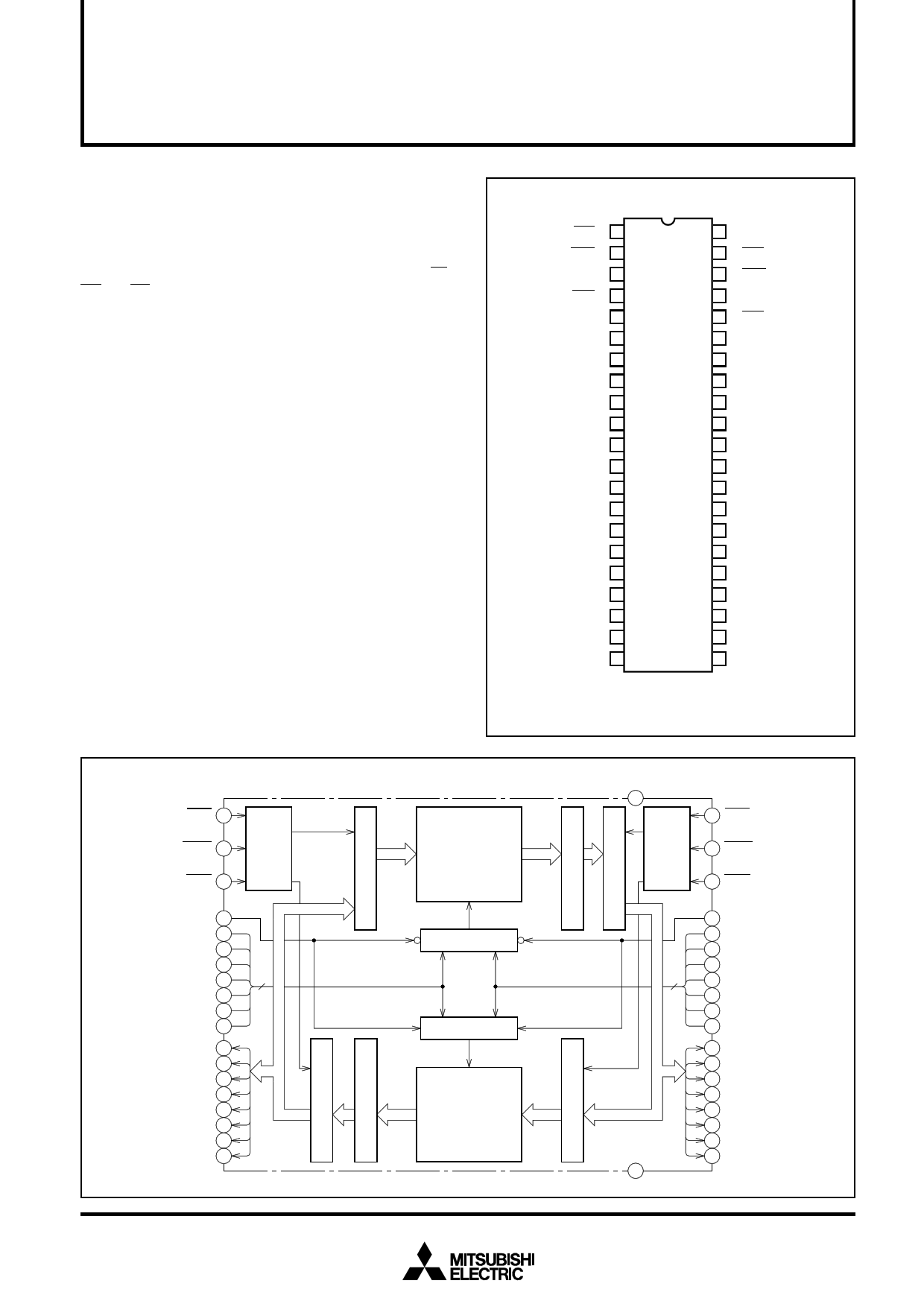
BLOCK DIAGRAM
CHIP SELECT CSA 1
INPUT
WRITE
WEA 2
ENABLE INPUT
OUTPUT
OEA 4
ENABLE INPUT
READ/
WRITE
CONTROL
CIRCUIT
A PORT
ADDRESS
INPUT
A PORT
DATA I/O
A7A 12
A0A 5
A1A 6
A2A 7
A3A 8
A4A 9
A5A 10
A6A 11
I/O0A 13
I/O1A 14
I/O2A 15
I/O3A 16
I/O4A 17
I/O5A 18
I/O6A 19
I/O7A 20
7
MEMORY AREA(1)
Write 128-WORD × 8-BIT
CONFIGURATION
0-127
ADDRESSES
Read
ROW/COLUMN
DECODER
A0A~A6A
ROW/COLUMN
DECODER
A0B~A6B
MEMORY AREA(2)
Read 128-WORD × 8-BIT Write
CONFIGURATION
128-255
ADDRESSES
VCC
42
READ/
WRITE
CONTROL
CIRCUIT
41 CSB CHIP
SELECT INPUT
40 WEB WRITE
ENABLE INPUT
38 OEB OUTPUT
ENABLE INPUT
7
21
GND
30 A7B
37 A0B
36 A1B
35 A2B
34 A3B
33 A4B
32 A5B
31 A6B
B PORT
ADDRESS
INPUT
22 I/O0B
23
24
I/O1B
I/O2B
25
26
I/O3B
I/O4B
B PORT
DATA I/O
27
28
I/O5B
I/O6B
29 I/O7B
1
1 page 
MITSUBISHI 〈DIGITAL ASSP〉
M66222SP/FP
128 × 8-BIT × 2 MAIL-BOX
SWITCHING CHARACTERISTICS (Ta = 0 ~ 70°C, VCC = 5V±10%, unless otherwise noted)
Read cycle
Symbol
tCR
ta(A)
ta(CS)
ta(OE)
tdis(CS)
tdis(OE)
ten(CS)
ten(OE)
tv(A)
Parameter
Read cycle time
Address access time
Chip select access time
Output enable access time
Output disable time after CS (Note 5)
Output disable time after OE (Note 5)
Output enable time after CS (Note 5)
Output enable time after OE (Note 5)
Data effective time after Address
Min.
70
5
5
10
Limits
Typ.
Max.
70
70
35
35
35
Unit
ns
ns
ns
ns
ns
ns
ns
ns
ns
TIMING REQUIREMENTS (Ta = 0 ~ 70°C, VCC = 5V±10%, unless otherwise noted)
Write cycle
Symbol
Parameter
Limits
Min. Typ.
tCW Write cycle time
70
tw(WE)
Write pulse width
45
tsu(A)1
Address setup time (for WE)
0
tsu(A)2
Address setup time (for CS)
0
tsu(A-WEH)
Address setup time for rise of WE
65
tsu(CS)
Chip select setup time
65
tsu(D)
Data setup time
40
th(D) Data hold time
0
trec(WE)
Write recovery time
0
tdis(WE)
Output disable time after WE (Note 5)
tdis(OE)
Output disable time after OE (Note 5)
ten(WE)
Output enable time after WE (Note 5)
0
ten(OE)
Output enable time after OE (Note 5)
5
Note 5: The time required for the output to change from a steady state to ±500mV under the load conditions shown in Figure 4.
This parameter is guaranteed but is not tested at shipment.
Max.
35
35
Unit
ns
ns
ns
ns
ns
ns
ns
ns
ns
ns
ns
ns
ns
5
5 Page | ||
| Páginas | Total 8 Páginas | |
| PDF Descargar | [ Datasheet M66222SP.PDF ] | |
Hoja de datos destacado
| Número de pieza | Descripción | Fabricantes |
| M66222SP | 128 x 8-BIT x 2 MAIL-BOX | Mitsubishi |
| Número de pieza | Descripción | Fabricantes |
| SLA6805M | High Voltage 3 phase Motor Driver IC. |
Sanken |
| SDC1742 | 12- and 14-Bit Hybrid Synchro / Resolver-to-Digital Converters. |
Analog Devices |
|
DataSheet.es es una pagina web que funciona como un repositorio de manuales o hoja de datos de muchos de los productos más populares, |
| DataSheet.es | 2020 | Privacy Policy | Contacto | Buscar |