|
|
|
PDF M29F016B Data sheet ( Hoja de datos )
| Número de pieza | M29F016B | |
| Descripción | 16 Mbit 2Mb x8 / Uniform Block Single Supply Flash Memory | |
| Fabricantes | ST Microelectronics | |
| Logotipo | ||
Hay una vista previa y un enlace de descarga de M29F016B (archivo pdf) en la parte inferior de esta página. Total 22 Páginas | ||
|
No Preview Available !
M29F016B
16 Mbit (2Mb x8, Uniform Block) Single Supply Flash Memory
s SINGLE 5V±10% SUPPLY VOLTAGE for
PROGRAM, ERASE and READ OPERATIONS
s ACCESS TIME: 55ns
s PROGRAMMING TIME
– 8µs by Byte typical
s 32 UNIFORM 64 Kbyte MEMORY BLOCKS
s PROGRAM/ERASE CONTROLLER
– Embedded Byte Program algorithm
– Embedded Multi-Block/Chip Erase algorithm
– Status Register Polling and Toggle Bits
– Ready/Busy Output Pin
s ERASE SUSPEND and RESUME MODES
– Read and Program another Block during
Erase Suspend
s TEMPORARY BLOCK UNPROTECTION
MODE
s UNLOCK BYPASS PROGRAM COMMAND
– Faster Production/Batch Programming
s LOW POWER CONSUMPTION
– Standby and Automatic Standby
s 100,000 PROGRAM/ERASE CYCLES per
BLOCK
s 20 YEARS DATA RETENTION
– Defectivity below 1 ppm/year
s ELECTRONIC SIGNATURE
– Manufacturer Code: 20h
– Device Code: ADh
TSOP40 (N)
10 x 20mm
44
1
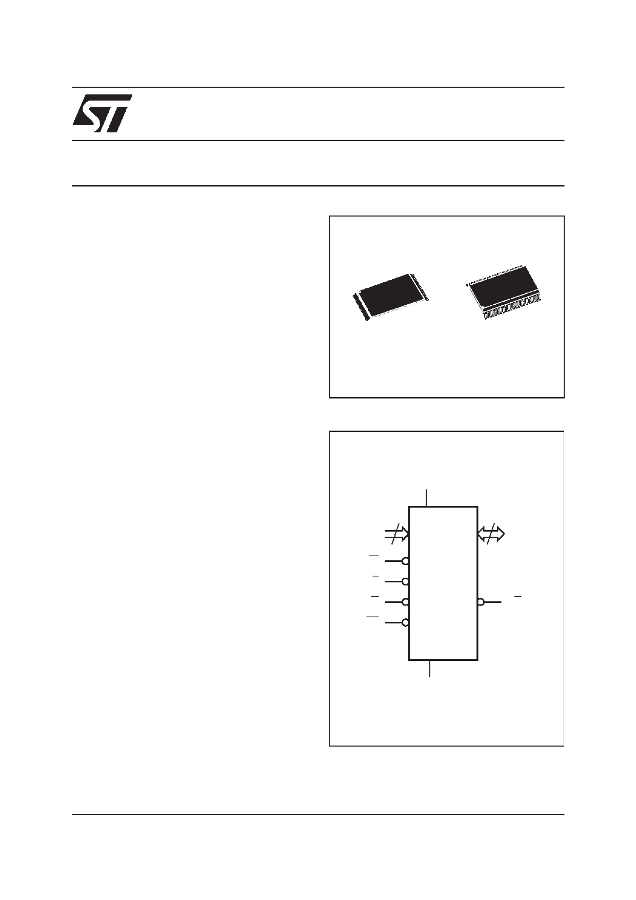
SO44 (M)
Figure 1. Logic Diagram
VCC
21
A0-A20
W
E
G
RP
M29F016B
8
DQ0-DQ7
RB
VSS
AI02964
March 2000
1/22
1 page 
M29F016B
After a Hardware Reset, Bus Read and Bus Write
operations cannot begin until Ready/Busy be-
comes high-impedance. See Table 14 and Figure
11, Reset/Temporary Unprotect AC Characteris-
tics.
During Program or Erase operations Ready/Busy
is Low, VOL. Ready/Busy will remain Low during
Read/Reset commands or Hardware Resets until
the memory is ready to enter Read mode.
The use of an open-drain output allows the Ready/
Busy pins from several memories to be connected
to a single pull-up resistor. A Low will then indicate
that one, or more, of the memories is busy.
VCC Supply Voltage. The VCC Supply Voltage
supplies the power for all operations (Read, Pro-
gram, Erase etc.).
The Command Interface is disabled when the VCC
Supply Voltage is less than the Lockout Voltage,
VLKO. This prevents Bus Write operations from ac-
cidentally damaging the data during power up,
power down and power surges. If the Program/
Erase Controller is programming or erasing during
this time then the operation aborts and the memo-
ry contents being altered will be invalid.
A 0.1µF capacitor should be connected between
the VCC Supply Voltage pin and the VSS Ground
pin to decouple the current surges from the power
supply. The PCB track widths must be sufficient to
carry the currents required during program and
erase operations, ICC4.
VSS Ground. The VSS Ground is the reference for
all voltage measurements.
BUS OPERATIONS
There are five standard bus operations that control
the device. These are Bus Read, Bus Write, Out-
put Disable, Standby and Automatic Standby. See
Table 4, Bus Operations, for a summary. Typically
glitches of less than 5ns on Chip Enable or Write
Enable are ignored by the memory and do not af-
fect bus operations.
Table 4. Bus Operations
Operation
E GW
Bus Read
Bus Write
Output Disable
Standby
Read Manufacturer
Code
VIL VIL VIH
VIL VIH VIL
X VIH VIH
VIH X
X
VIL VIL VIH
Read Device Code
Note: X = VIL or VIH.
VIL VIL VIH
Bus Read. Bus Read operations read from the
memory cells, or specific registers in the Com-
mand Interface. A valid Bus Read operation in-
volves setting the desired address on the Address
Inputs, applying a Low signal, VIL, to Chip Enable
and Output Enable and keeping Write Enable
High, VIH. The Data Inputs/Outputs will output the
value, see Figure 8, Read Mode AC Waveforms,
and Table 11, Read AC Characteristics, for details
of when the output becomes valid.
Bus Write. Bus Write operations write to the
Command Interface. A valid Bus Write operation
begins by setting the desired address on the Ad-
dress Inputs. The Address Inputs are latched by
the Command Interface on the falling edge of Chip
Enable or Write Enable, whichever occurs last.
The Data Inputs/Outputs are latched by the Com-
mand Interface on the rising edge of Chip Enable
or Write Enable, whichever occurs first. Output En-
able must remain High, VIH, during the whole Bus
Write operation. See Figures 9 and 10, Write AC
Waveforms, and Tables 12 and 13, Write AC
Characteristics, for details of the timing require-
ments.
Output Disable. The Data Inputs/Outputs are in
the high impedance state when Output Enable is
High, VIH.
Standby. When Chip Enable is High, VIH, the
Data Inputs/Outputs pins are placed in the high-
impedance state and the Supply Current is re-
duced to the Standby level.
When Chip Enable is at VIH the Supply Current is
reduced to the TTL Standby Supply Current, ICC2.
To further reduce the Supply Current to the CMOS
Standby Supply Current, ICC3, Chip Enable should
be held within VCC ± 0.2V. For Standby current
levels see Table 10, DC Characteristics.
During program or erase operations the memory
will continue to use the Program/Erase Supply
Current, ICC4, for Program or Erase operations un-
til the operation completes.
Address Inpu ts
Cell Address
Command Address
X
X
A0 = VIL, A1 = VIL, A9 = VID,
Others VIL or VIH
A0 = VIH, A1 = VIL, A9 = VID,
Others VIL or VIH
Data
Inputs/Outpu ts
Data Output
Data Input
Hi-Z
Hi-Z
20h
ADh
5/22
5 Page 
Figure 4. Data Polling Flowchart
START
READ DQ5 & DQ7
at VALID ADDRESS
DQ= 7 YES
DATA
NO
NO DQ5
=1
YES
READ DQ7
at VALID ADDRESS
DQ7
=
YES
DATA
NO
FAIL
PASS
AI03598
M29F016B
Figure 5. Data Toggle Flowchart
START
READ
DQ5 & DQ6
READ DQ6
DQ= 6
NO
TOGGLE
YES
NO DQ5
=1
YES
READ DQ6
TWICE
DQ= 6
NO
TOGGLE
YES
FAIL
PASS
AI01370B
Erase Timer Bit (DQ3). The Erase Timer Bit can
be used to identify the start of Program/Erase
Controller operation during a Block Erase com-
mand.
Once the Program/Erase Controller starts erasing
the Erase Timer Bit is set to ’1’. Before the Pro-
gram/Erase Controller starts the Erase Timer Bit is
set to ’0’ and additional blocks to be erased may
be written to the Command Interface. The Erase
Timer Bit is output on DQ3 when the Status Reg-
ister is read.
Alternative Toggle Bit (DQ2). The Alternative
Toggle Bit can be used to monitor the Program/
Erase controller during Erase operations. The Al-
ternative Toggle Bit is output on DQ2 when the
Status Register is read.
During Chip Erase and Block Erase operations the
Toggle Bit changes from ’0’ to ’1’ to ’0’, etc., with
successive Bus Read operations from addresses
within the blocks being erased. Once the operation
completes the memory returns to Read mode.
During Erase Suspend the Alternative Toggle Bit
changes from ’0’ to ’1’ to ’0’, etc. with successive
Bus Read operations from addresses within the
blocks being erased. Bus Read operations to ad-
dresses within blocks not being erased will output
the memory cell data as if in Read mode.
After an Erase operation that causes the Error Bit
to be set the Alternative Toggle Bit can be used to
identify which block or blocks have caused the er-
ror. The Alternative Toggle Bit changes from ’0’ to
’1’ to ’0’, etc. with successive Bus Read Opera-
tions from addresses within blocks that have not
erased correctly. The Alternative Toggle Bit does
not change if the addressed block has erased cor-
rectly.
11/22
11 Page | ||
| Páginas | Total 22 Páginas | |
| PDF Descargar | [ Datasheet M29F016B.PDF ] | |
Hoja de datos destacado
| Número de pieza | Descripción | Fabricantes |
| M29F016B | 16 Mbit 2Mb x8 / Uniform Block Single Supply Flash Memory | ST Microelectronics |
| M29F016D | 16 Megabit (2 M x 8-Bit) CMOS 5.0 Volt-only / Uniform Sector Flash Memory | Advanced Micro Devices |
| Número de pieza | Descripción | Fabricantes |
| SLA6805M | High Voltage 3 phase Motor Driver IC. |
Sanken |
| SDC1742 | 12- and 14-Bit Hybrid Synchro / Resolver-to-Digital Converters. |
Analog Devices |
|
DataSheet.es es una pagina web que funciona como un repositorio de manuales o hoja de datos de muchos de los productos más populares, |
| DataSheet.es | 2020 | Privacy Policy | Contacto | Buscar |