|
|
|
PDF LC99012A-S Data sheet ( Hoja de datos )
| Número de pieza | LC99012A-S | |
| Descripción | Black-and-White CCD Timing Generator | |
| Fabricantes | Sanyo | |
| Logotipo | ||
Hay una vista previa y un enlace de descarga de LC99012A-S (archivo pdf) en la parte inferior de esta página. Total 6 Páginas | ||
|
No Preview Available !
Ordering number : EN*5281A
CMOS LSI
LC99012A-S
Black-and-White CCD Timing Generator
Preliminary
Overview
The LC99012A-S is a timing generator for the 1/5-inch
LC9947G and LC9948G and the 1/6-inch LC9949G
black-and-white CCD image sensors.
Features
• 5 V single-voltage power supply
• Generates all pulses required for CCD drivers.
• Generates all pulses required for video signal
processing.
• Built-in synchronizing signal generator that supports
both EIA and CCIR.
• Includes buffer circuits for directly driving the CCD
horizontal transfer and reset gates.
• Includes light metering and control systems for an
automatic electronic iris function.
• Fixed rate-of-change control allows a smooth electronic
iris function to be implemented (an iris state output is
provided).
• Supports AGC control and a light metering mode that
compensates for backlighting.
• Selectable CCD storage mode (non-interlaced or
interlaced)
• Selectable TV scan mode (non-interlaced or interlaced)
• Allows all types of external synchronization.
• Built-in EXT-C.SYNC sync separator circuit
• Built-in phase comparator for external synchronization
• Control from external electronic shutter pulses and
frame shift pulses supports one-shot imaging.
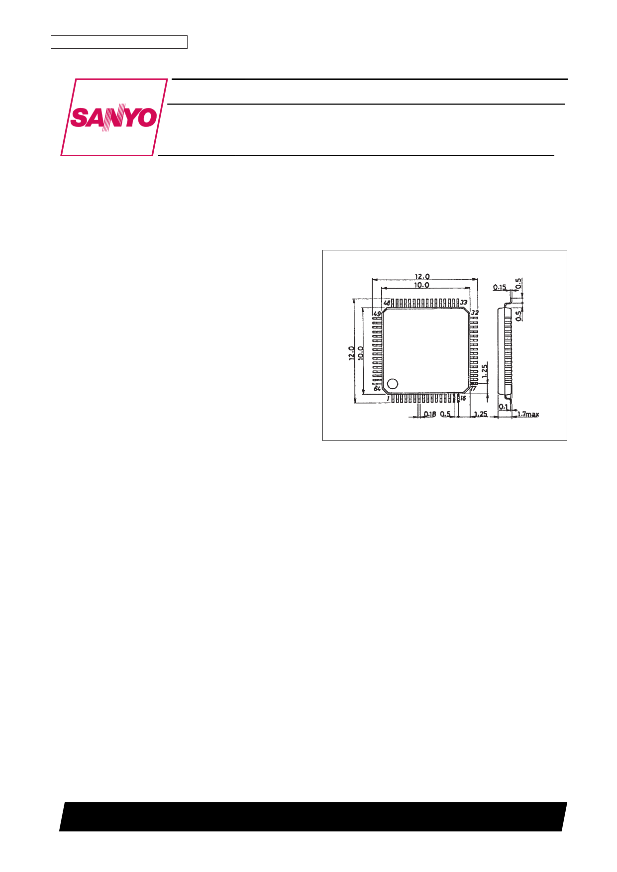
• Package: 0.5 mm lead pitch flat package (SQFP-64)
• Flickerless function
• Sensitivity-increasing function
Package Dimensions
unit: mm
3190-SQFP64
[LC99012A-S]
SANYO: SQFP64
SANYO Electric Co.,Ltd. Semiconductor Bussiness Headquarters
TOKYO OFFICE Tokyo Bldg., 1-10, 1 Chome, Ueno, Taito-ku, TOKYO, 110-8534 JAPAN
22896HA (OT) No. 5281-1/6
1 page 
LC99012A-S
Pin Functions
Pin No.
Symbol
I/O
Function
1 GND
2
PCO
O Phase comparator output
3 AI I PCO output signal low-pass filter amplifier input
4 AO O PCO output signal low-pass filter amplifier output
Reference clock input (resonator inverter input)
5
CKI
I
LC9947G: 28.63636 MHz
LC9948G: 28.375 MHz
LC9949G: 14.31818 MHz
6
CKO
O Resonator inverter output
Low/open: CCD interlaced storage mode
7
CCDSCAN
I High: CCD non-interlaced storage mode
Low/open: C.SYNC interlaced mode
8
SSGSCAN
I High: C.SYNC non-interlaced mode
LC9947G/9949G: 14.31818 MHz
9
CLK14M
O LC9948G: 14.1875 MHz
10 HD O HD output
11 VD O VD output
Field identifier signal
High: odd
12 FLD O Low: even
Must be tied high if SSGSCAN is high.
13 VDD
14
KISYU
I Must be tied high when used with the LC9949G. Otherwise must be tied low.
15 HR I Horizontal reset, C.SYNC reset, and vertical reset pulse input
16 VR I Vertical reset pulse input and external synchronization mode setup
17 GND
18
SELMET1
I Light metering mode control
19
SELMET2
I Light metering mode control
20
EXT1
I External synchronization mode control
21
EXT2
I External synchronization mode control
22
EXT3
I CCD drive external control mode control
23
EXT4
I CCD drive external control mode control
24
VDD
I
Normally used to control the electronic iris step (rate of change)
25
STEPSTOP
I/O Low: 1/8
Hifh: 1/16
Sensitivity increasing switch
26
SENS
I Low/open: normal
High: Increased sensitivity mode
Increased sensitivity mode type switching
27
MSENS
I Low or open: In field units
High: In single scan line (1H) units
Flickerless mode* switch
28
FLESS
I Low: Flickerless mode
High/open: normal
CCD storage mode control
29
STR
I This pin must be left open or tied high when the LC99012A-S is used with an LC9947G/49G, and must
be tied low when used with an LC9948G.
30
NSUB3
O CCD NSUB pulses
31
NSUB2
O CCD NSUB pulses
32
NSUB1
O CCD NSUB pulses
Low: test mode
33
TEST
I High/open: normal operating mode
34 VI1 O CCD imaging block transfer clock (ø1)
35 VI3 O CCD imaging block transfer clock (ø3)
36 VI2 O CCD imaging block transfer clock (ø2)
37 VI4 O CCD imaging block transfer clock (ø4)
38 VS4 O CCD imaging block transfer clock (øS4)
Note: * Flickerless mode can be used when the auto-iris function is off, i.e. when EXT3 is high and EXT4 is low.
Continued on next page.
No. 5281-5/6
5 Page | ||
| Páginas | Total 6 Páginas | |
| PDF Descargar | [ Datasheet LC99012A-S.PDF ] | |
Hoja de datos destacado
| Número de pieza | Descripción | Fabricantes |
| LC99012A-S | Black-and-White CCD Timing Generator | Sanyo |
| Número de pieza | Descripción | Fabricantes |
| SLA6805M | High Voltage 3 phase Motor Driver IC. |
Sanken |
| SDC1742 | 12- and 14-Bit Hybrid Synchro / Resolver-to-Digital Converters. |
Analog Devices |
|
DataSheet.es es una pagina web que funciona como un repositorio de manuales o hoja de datos de muchos de los productos más populares, |
| DataSheet.es | 2020 | Privacy Policy | Contacto | Buscar |