|
|
PDF LC89975M Data sheet ( Hoja de datos )
| Número de pieza | LC89975M | |
| Descripción | PAL-Format Delay Line | |
| Fabricantes | Sanyo | |
| Logotipo |  |
|
Hay una vista previa y un enlace de descarga de LC89975M (archivo pdf) en la parte inferior de esta página. Total 7 Páginas | ||
|
No Preview Available !
Ordering number : EN*5391
NMOS + CCD
LC89975M
PAL-Format Delay Line
Preliminary
Overview
The LC89975M is a lower-cost PAL-Format CCD delay
line based on the LC89970M, with the sizes of chip and
package miniaturized and the external parts count reduced.
Features
• 5 V single-voltage power supply
• On-chip 3× PLL circuit for 3·fsc operation from an fsc
(4.43 MHz) input
• Supports PAL/GBI and 4.43 NTSC systems, selected by
a control pin input
• Includes an on-chip comb filter for chrominance signal
crosstalk exclusion. This adjustment-free circuit
provides high-precision comb characteristics.
• Peripheral circuits included on chip to allow operation
with minimal external circuits.
• Positive-phase signal input, positive phase signal output
(luminance signal)
Functions
• CCD shift register (for chrominance and luminance
signals)
• CCD drive circuit
• Circuit for switching the number of CCD stages
• CCD signal addition circuit
• Auto-bias circuit
• Sync tip clamping circuit (luminance signal)
• Center bias circuit (chrominance signal)
• Sample-and-hold circuit
• PLL 3× circuit
• 3·fsc clock output circuit
• RD voltage generation step-up circuit
Package Dimensions
unit: mm
3111-MFP14S
[LC89975M]
SANYO: MFP14S
Specifications
Absolute Maximum Ratings at Ta = 25°C
Parameter
Supply voltage
Allowable power dissipation
Operating temperature
Storage temperature
Symbol
VDD
Pdmax
Topr
Tstg
Conditions
Ratings
–0.3 to +6.0
250
–10 to +60
–55 to +150
Unit
V
mW
°C
°C
Recommended Conditions at Ta = 25°C
Parameter
Symbol
Supply voltage
Clock input amplitude
Clock frequency
Chrominance signal input amplitude
Luminance signal input amplitude
VDD
VCLK
FCLK
VIN-C
VIN-Y
Sine wave
Conditions
min
4.75
300
—
—
—
typ
5.00
500
4.43361875
350
400
max
5.25
1000
—
500
572
Unit
V
mVp-p
MHz
mVp-p
mVp-p
SANYO Electric Co.,Ltd. Semiconductor Bussiness Headquarters
TOKYO OFFICE Tokyo Bldg., 1-10, 1 Chome, Ueno, Taito-ku, TOKYO, 110-0005 JAPAN
41596HA (OT) No. 5391-1/7
1 page 
LC89975M
Test Conditions
1. Power-supply current with no input signal applied
2. Pin output voltage with no input signal applied (center bias voltage)
3. Measure the C-OUT output when 350-mVp-p sine wave signals are input to C-IN1 and C-IN2.
GVC
=
20
log
C-OUT output [mVp-p]
350 [mVp-p]
[dB]
Measured frequencies
GVC-1
GVC-2
4.429662 MHz
4.425694 MHz
(PAL/GBI)
(4.43 NTSC)
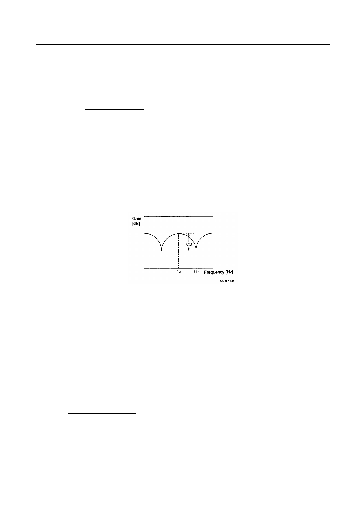
4. Measure the comb depth from the C-OUT output when 350-mVp-p sine wave signals of frequency fa are input to C-
IN1 and C-IN2 and when signals of frequency fb are input.
CD = 20 log
The C-OUT output for an fb input [mVp-p]
The C-OUT output for an fa input [mVp-p]
[dB]
Measured frequencies
CD-1
CD-2
fa
4.429662 MHz
4.425694 MHz
fb
4.425756 MHz
4.417819 MHz
(PAL/GBI)
(4.43 NTSC)
5. Measure the C-OUT output when 200-mVp-p sine wave signals are input to C-IN1 and C-IN2 and when 500-mVp-p
sine wave signals are input and calculate the gain difference.
( )LNC = 20 log
Output
for
a
500-mVp-p input
500 [mVp-p]
[mVp-p]
/
Output
for
a
200-mVp-p input
200 [mVp-p]
[mVp-p]
[dB]
Measured frequencies
LNC-1
LNC-2
4.429662 MHz
4.425694 MHz
(PAL/GBI)
(4.43 NTSC)
6. Measure the 3·fsc (13.3 MHz) and fsc (4.43 MHz) components in the C-OUT output with no input signal applied.
7. Measure the noise in the C-OUT output with no input signal applied.
Set up the noise meter with a 200-kHz high-pass filter and a 5-MHz low-pass filter.
8. Let V1 be the C-OUT output when 350-mVp-p sine wave signals are input to C-IN1 and C-IN2 with SW3 in the a
position, and V2 be the C-OUT output with SW3 in the b position.
ZOC =
V2 [mVp-p] – V1 [mVp-p]
V1 [mVp-p]
× 500 [Ω]
Measured frequencies
ZOC-1
ZOC-2
4.429662 MHz
4.425694 MHz
(PAL/GBI)
(4.43 NTSC)
No. 5391-5/7
5 Page | ||
| Páginas | Total 7 Páginas | |
| PDF Descargar | [ Datasheet LC89975M.PDF ] | |
Hoja de datos destacado
| Número de pieza | Descripción | Fabricantes |
| LC89975M | PAL-Format Delay Line | Sanyo |
| Número de pieza | Descripción | Fabricantes |
| SLA6805M | High Voltage 3 phase Motor Driver IC. |
Sanken |
| SDC1742 | 12- and 14-Bit Hybrid Synchro / Resolver-to-Digital Converters. |
Analog Devices |
|
DataSheet.es es una pagina web que funciona como un repositorio de manuales o hoja de datos de muchos de los productos más populares, |
| DataSheet.es | 2020 | Privacy Policy | Contacto | Buscar |
