|
|
|
PDF LC895125Q Data sheet ( Hoja de datos )
| Número de pieza | LC895125Q | |
| Descripción | CD-ROM Driver with On-Chip SCSI Interface and Subcode Functions | |
| Fabricantes | Sanyo | |
| Logotipo | ||
Hay una vista previa y un enlace de descarga de LC895125Q (archivo pdf) en la parte inferior de esta página. Total 11 Páginas | ||
|
No Preview Available !
Ordering number : EN*5241
Preliminary
CMOS LSI
LC895125Q, 895125W
CD-ROM Driver with On-Chip SCSI Interface and
Subcode Functions
Functions
CD-ROM ECC function, subcode read function, SCSI
interface
Features
• On-chip SCSI interface (with built-in SCAM selection
register)
• Supports 8× playback - Using ×16 80-ns DRAMs
• Supports 4× playback - Using ×16 80-ns DRAMs or ×8
70-ns DRAMs
• Transfer rates: 10 MB/s (synchronous), 5 MB/s
(asynchronous) using ×16 80-ns DRAMs*1
• Transfer rates: 8.467 MB/s (synchronous), 4.2336 MB/s
(asynchronous) using ×8 70-ns DRAMs*2
• Supports the connection of up to 32 Mb of buffer RAM
(using DRAM)
• The user can freely set the CD main channel, C2 flag,
and other areas in buffer RAM.
• Batch transfer function (transfers the CD main channel
and C2 flag data in a single operation)
• Multi-block transfer function (automatically transfers
multiple blocks in a single operation)
• High-speed transfer mode supports a 10-MB/s
(synchronous) transfer rate using ×8 80-ns DRAMs
• Subcode ECC function
Note: 1. For speeds up to 8× speed, use a SCSI master
clock frequency of 20 MHz.
Note: 2. For speeds up to 4× speed, use a SCSI master
clock frequency of 16.9344 MHz.
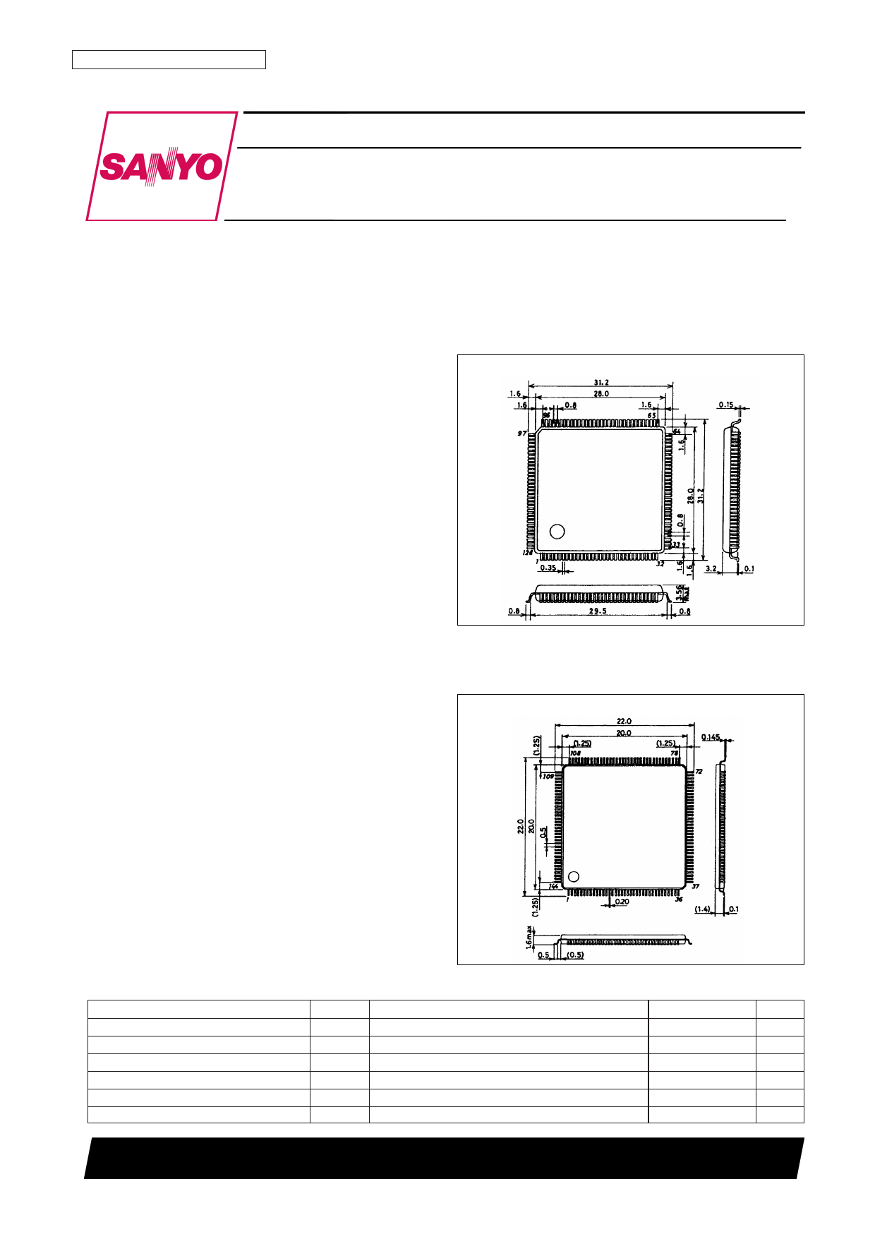
Package Dimensions
unit: mm
3182-QIP128E
[LC895125Q]
unit: mm
3214-SQFP144
[LC895125W]
SANYO: QIP128E
Specifications
Absolute Maximum Ratings at VSS = 0 V
Parameter
Maximum supply voltage
I/O voltages
Allowable power dissipation
Operating temperature
Storage temperature
Soldering heat resistance (pins only)
Symbol
VDD max
VI, VO
Pd max
Topr
Tstg
Ta = 25°C
Ta = 25°C
Ta ≤ 70°C
10 seconds
Conditions
SANYO: SQFP144
Ratings
–0.3 to +7.0
–0.3 to VDD + 0.3
450
–30 to +70
–55 to +125
260
Unit
V
V
mW
°C
°C
°C
SANYO Electric Co.,Ltd. Semiconductor Bussiness Headquarters
TOKYO OFFICE Tokyo Bldg., 1-10, 1 Chome, Ueno, Taito-ku, TOKYO, 110-0005 JAPAN
22896HA (OT) No. 5241-1/11
1 page 
LC895125Q, 895125W
Continued from preceding page.
Type: I: Input pin, O: Output pin, B: Bidirectional pin, P: Power supply pin, NC: No connection pin
Pin No.
Symbol
Type
Function
51
ZRD
I Microcontroller data read signal input
52
ZWR
I Microcontroller data write signal input
53
ZCS
I Register chip select signal from the microcontroller
54
SUA0
I
55
SUA1
I
56
SUA2
I
57
SUA3
I Microcontroller register selection signals
58
SUA4
I
59
SUA5
I
60
SUA6
I
61
VSS0
P
62
X1EN
I Selection pin that must be set to 1 when XTALCK1 is used.
63
XTALCK1
I SCSI block oscillator circuit input. Selected by X1EN.
64
XTAL1
O SCSI block oscillator circuit output.
65
VDD
P
66
VSS1
P
67
DB0
B
SCSI connection
68
DB1
B
69
VSS1
P
70
DB2
B
SCSI connection
71
DB3
B
72
VDD
P
73
VSS1
P
74
DB4
B
SCSI connection
75
DB5
B
76
VSS1
P
77
DB6
B
SCSI connection
78
DB7
B
79
VSS1
P
80
DBP
B SCSI connection
81
VSS1
P
82
ATN
B SCSI connection
83
VDD
P
84
BSY
B
SCSI connection
85
ACK
B
86
VSS1
P
87
RST
B
SCSI connection
88
MSG
B
89
VDD
P
90 SEL B
SCSI connection
91 C/D B
92
VSS1
P
93
REQ
B
SCSI connection
94 I/O B
95
VSS1
P
96
VDD
P
97
VSS0
P
98 NC
99
VSS0
P
100 VSS0 P
Note: 1. NC pins must be left open. Do not connect any signal to these pins.
2. Pin names that start with Z are negative-logic signals.
3. VSS0 is the logic system ground and VSS1 is the SCSI interface ground.
4. Applications that use DRAM must insert resistors in the CAS and RAS lines, connect capacitors between these lines and ground, and take any
other measures necessary to prevent undershoot in the DRAM related circuits.
5. Since these circuits include buffers that sink 48 mA, adequate noise prevention measures must be applied.
Continued on next page.
No. 5241-5/11
5 Page 
LC895125Q, 895125W
5. CD DSP Data Pins
• BCK, SDATA, LRCK, C2PO (input)
The LC895125 reads in CD-ROM data over these pins connected to a CD DSP.
C2PO is the C2 flag pin.
6. Other Pins
• ZRESET (input)
Reset input to the LC895125. The LC895125 is reset by a low-level input.
This pin must be held low for a period of at least 1 µs when power is first applied.
• XTALCK0, XTAL0
The main clock for the ECC and SCSI blocks. These pins support frequencies from 16.9344 to 25 MHz.
When a double-frequency input is used, these pins accept frequencies up to 38 MHz.
Use a double-frequency input when a ceramic oscillator and DRAM are used.
(This is because the internal clock must have a 50% duty.)
An external clock may input to the XTALCK pin.
The SCSI block main clock can also be provided from XTALCK1 and XTAL1 if so specified by the setting of
X1EN (pin 89).
• XTALCK1, XTAL1
The main clock for the ECC and SCSI blocks. These pins are enabled for oscillator operation by setting X1EN (pin
89). The LC895125 is designed so that the ECC and SCSI blocks can also be operated asynchronously.
This means that precise 10-MB/s synchronous transfers can be achieved by providing a 20-MHz input to
XTALCK1 and XTAL1.
A ceramic oscillator may be used here since only the rising edge of this signal is used.
In applications that do not use these pins, XTALCK1 must be tied to VSS and XTAL1 must be left open.
• X1EN (input)
Set this pin to 1 to us use XTALCK1 and XTAL1 for the SCSI block main clock.
Set this pin to 0 to drive both the ECC and SCSI blocks from XTALCK0 and XTAL0.
• MCK (output)
Outputs either the XTALCK0 frequency or that frequency divided by 2. This pin’s output can also be stopped if
desired.
s No products described or contained herein are intended for use in surgical implants, life-support systems, aerospace
equipment, nuclear power control systems, vehicles, disaster/crime-prevention equipment and the like, the failure of
which may directly or indirectly cause injury, death or property loss.
s Anyone purchasing any products described or contained herein for an above-mentioned use shall:
Accept full responsibility and indemnify and defend SANYO ELECTRIC CO., LTD., its affiliates, subsidiaries and
distributors and all their officers and employees, jointly and severally, against any and all claims and litigation and all
damages, cost and expenses associated with such use:
Not impose any responsibility for any fault or negligence which may be cited in any such claim or litigation on
SANYO ELECTRIC CO., LTD., its affiliates, subsidiaries and distributors or any of their officers and employees
jointly or severally.
s Information (including circuit diagrams and circuit parameters) herein is for example only; it is not guaranteed for
volume production. SANYO believes information herein is accurate and reliable, but no guarantees are made or implied
regarding its use or any infringements of intellectual property rights or other rights of third parties.
This catalog provides information as of February, 1996. Specifications and information herein are subject to
change without notice.
PS No. 5241-11/11
11 Page | ||
| Páginas | Total 11 Páginas | |
| PDF Descargar | [ Datasheet LC895125Q.PDF ] | |
Hoja de datos destacado
| Número de pieza | Descripción | Fabricantes |
| LC895125Q | CD-ROM Driver with On-Chip SCSI Interface and Subcode Functions | Sanyo |
| LC895125W | CD-ROM Driver with On-Chip SCSI Interface and Subcode Functions | Sanyo |
| Número de pieza | Descripción | Fabricantes |
| SLA6805M | High Voltage 3 phase Motor Driver IC. |
Sanken |
| SDC1742 | 12- and 14-Bit Hybrid Synchro / Resolver-to-Digital Converters. |
Analog Devices |
|
DataSheet.es es una pagina web que funciona como un repositorio de manuales o hoja de datos de muchos de los productos más populares, |
| DataSheet.es | 2020 | Privacy Policy | Contacto | Buscar |