|
|
|
PDF LC662304A Data sheet ( Hoja de datos )
| Número de pieza | LC662304A | |
| Descripción | Four-Bit Single-Chip Microcontroller with 16 KB of On-Chip EPROM | |
| Fabricantes | Sanyo | |
| Logotipo | ||
Hay una vista previa y un enlace de descarga de LC662304A (archivo pdf) en la parte inferior de esta página. Total 25 Páginas | ||
|
No Preview Available !
Preliminary
No. 5483
CMOS LSI
LC662304A, 662306A, 662308A, 662312A, 662316A
Four-Bit Single-Chip Microcontrollers
with 4, 6, 8, 12, and 16 KB of On-Chip ROM
Overview
The LC662304A, LC662306A, LC662308A, LC662312A,
and LC662316A are 4-bit CMOS microcontrollers that
integrate on a single chip all the functions required in a
special-purpose telephone controller, including ROM,
RAM, I/O ports, a serial interface, a DTMF generator,
timers, and interrupt functions. These microcontrollers are
available in a 42-pin package.
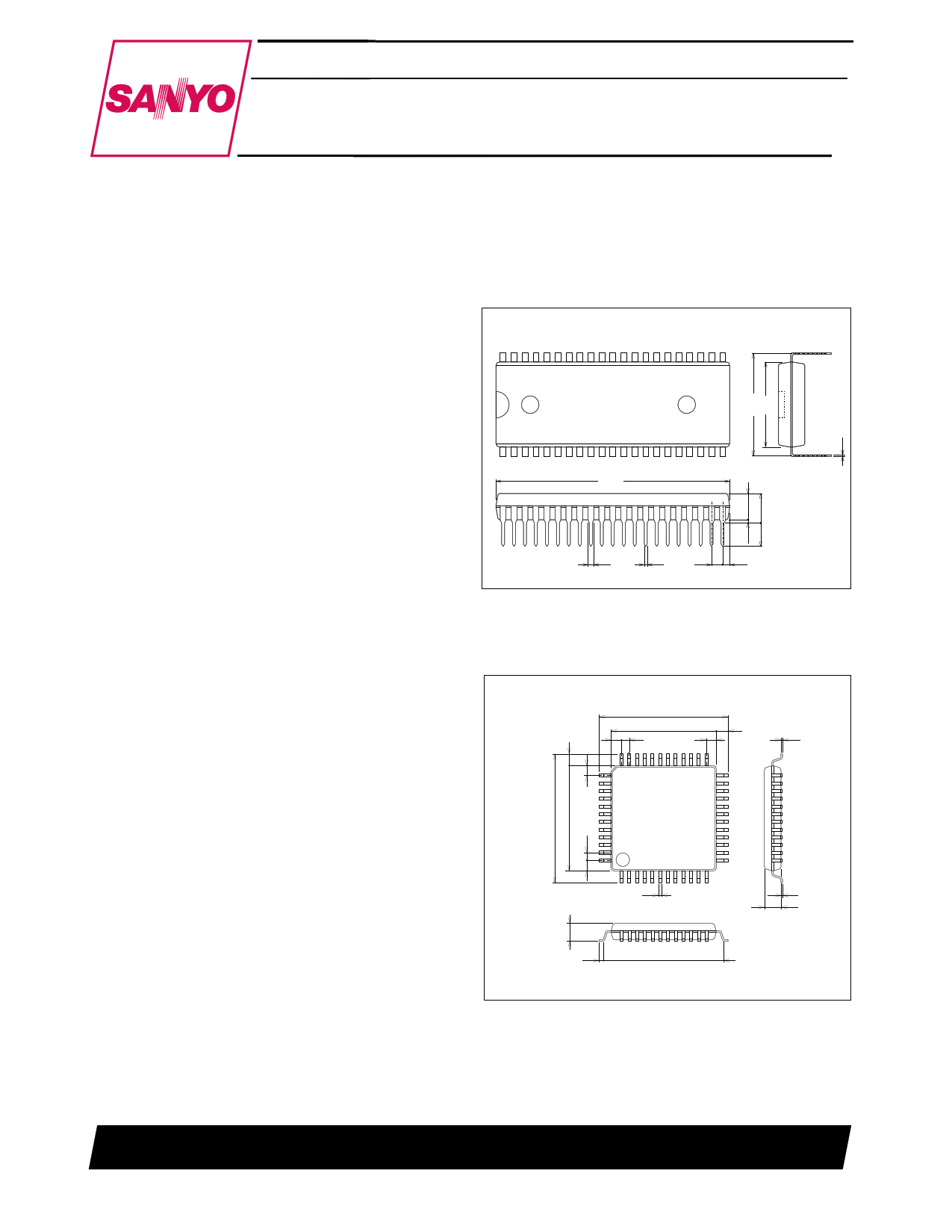
Package Dimensions
unit: mm
3025B-DIP42S
[LC662304A/662306A/662308A/662312A/662316A]
42 22
Features and Functions
• On-chip ROM capacities of 4, 6, 8, 12, and 16 kilobytes,
and an on-chip RAM capacity of 512 × 4 bits.
• Fully supports the LC66000 Series common instruction
set (128 instructions).
• I/O ports: 36 pins
• DTMF generator
This microcontroller incorporates a circuit that can
generate two sine wave outputs, DTMF output, or a
melody output for software applications.
• 8-bit serial interface: one circuit
• Instruction cycle time: 0.95 to 10 µs (at 3.0 to 5.5 V)
• Powerful timer functions and prescalers
— Time limit timer, event counter, pulse width
measurement, and square wave output using a 12-bit
timer.
— Time limit timer, event counter, PWM output, and
square wave output using an 8-bit timer.
— Time base function using a 12-bit prescaler.
• Powerful interrupt system with 10 interrupt factors and 7
interrupt vector locations.
— External interrupts: 3 factors/3 vector locations
— Internal interrupts: 4 factors/4 vector locations
(Waveform output internal interrupts: 3 factors and 1
vector; shared with external expansion interrupts)
• Flexible I/O functions
Selectable options include 20-mA drive outputs, inverter
circuits, pull-up and open drain circuits.
• Optional runaway detection function (watchdog timer)
• 8-bit I/O functions
• Power saving functions using halt and hold modes.
• Packages: DIP42S, QIP48E (QFP48E)
• Evaluation LSIs: LC66599 (evaluation chip) +
EVA800/850-TB662YXX2
LC66E2316(on-chip EPROM microcontroller)
1
37.9
21
0.95 0.48 1.78 1.15
SANYO: DIP42S
unit: mm
3156-QFP48E
[LC662304A/662306A/662308A/662312A/662316A]
17.2
14.0
1.5 1.0
36
37
1.6
1.5
25
24
0.15
48
1
0.35
13
12
0.1
2.70
(STAND OFF)
0.8 15.6
SANYO: QFP48E
SANYO Electric Co.,Ltd. Semiconductor Bussiness Headquarters
TOKYO OFFICE Tokyo Bldg., 1-10, 1 Chome, Ueno, Taito-ku, TOKYO, 110 JAPAN
22897HA (OT) No. 5483-1/25
1 page 
LC662304A, 662306A, 662308A, 662312A, 662316A
Pin Function Overview
Pin I/O
Overview
Output driver type
Options
State after a Standby mode
reset
operation
P00
P01
P02
P03
I/O ports P00 to P03
• Input or output in 4-bit or 1-bit units
I/O • P00 to P03 support the halt mode
control function (This function can be
specified in bit units.)
• Pch: Pull-up MOS type
• Nch: Intermediate sink current
type
• Pull-up MOS or
Nch OD output
• Output level on
reset
High or low
(option)
Hold mode:
Output off
Halt mode:
Output
retained
P10
P11
P12
I/O
I/O ports P10 to P13
Input or output in 4-bit or 1-bit units
P13
• Pch: Pull-up MOS type
• Nch: Intermediate sink current
type
• Pull-up MOS or
Nch OD output
• Output level on
reset
P20/SI0
P21/SO0
P22/SCK0
P23/INT0
I/O ports P20 to P23
• Input or output in 4-bit or 1-bit units
• P20 is also used as the serial input SI0
I/O
pin.
• P21 is also used as the serial output
SO0 pin.
• P22 is also used as the serial clock
SCK0 pin.
• P23 is also used as the INT0 interrupt
• Pch: CMOS type
• Nch: Intermediate sink current
type
• Nch: +12-V handling when
OD option selected
CMOS or Nch OD
output
request pin, and also as the timer 0
event counting and pulse width
measurement input.
High or low
(option)
Hold mode:
Output off
Halt mode:
Output
retained
Hold mode:
Output off
H
Halt mode:
Output
retained
I/O ports P30 to P32
• Input or output in 3-bit or 1-bit units
P30/INT1
P31/POUT0
P32/POUT1
I/O
• P30 is also used as the INT1 interrupt
request.
• P31 is also used for the square wave
output from timer 0.
• P32 is also used for the square wave
and PWM output from timer 1.
• Pch: CMOS type
• Nch: Intermediate sink current
type
• Nch: +12-V handling when
OD option selected
CMOS or Nch OD
output
• P31 and P32 also support 3-state
outputs.
Hold mode:
Output off
H
Halt mode:
Output
retained
P33/HOLD
Hold mode control input
• Hold mode is set up by the HOLD
instruction when HOLD is low.
• In hold mode, the CPU is restarted by
setting HOLD to the high level.
I
• This pin can be used as input port P33
along with P30 to P32.
• When the P33/HOLD pin is at the low
level, the CPU will not be reset by a
low level on the RES pin. Therefore,
applications must not set P33/HOLD
low when power is first applied.
P40/INV0I
P41/INV0O
P42/INV1I
P43/INV1O
I/O ports P40 to P43
I/O
• Input or output in 4-bit or 1-bit units
• Input or output in 8-bit units when used
in conjunction with P50 to P53.
• Can be used for output of 8-bit ROM
data when used in conjunction with
P50 to P53.
• Pch: Pull-up MOS type
• CMOS type when the inverter
circuit option is selected
• Nch: Intermediate sink current
type
• Pull-up MOS or
Nch OD output
• Output level on
reset
• Inverter circuit
• Dedicated inverter circuit (option)
High or low
or inverter
I/O (option)
Hold mode:
Port output
off, inverter
output off
Halt mode:
Port output
retained,
inverter
output
continues
Continued on next page.
No. 5483-5/25
5 Page 
LC662304A, 662306A, 662308A, 662312A, 662316A
Continued from preceding page.
ROM area
3FFEH
3FFFH
Bit Option specified
7
6
5
4
Reserved. Must be set to predefined data values.
3
2
1
0
7
6
5
4
Reserved. Must be set to predefined data values.
3
2
1
0
Option/data relationship
This data is generated by the assembler.
If the assembler is not used, set this data to ‘00’.
This data is generated by the assembler.
If the assembler is not used, set this data to ‘00’.
Specifications
Absolute Maximum Ratings at Ta = 25°C, VSS = 0 V
Parameter
Symbol
Conditions
Ratings
Unit Note
Maximum supply voltage
Input voltage
Output voltage
VDD max
VIN1
VIN2
VOUT1
VOUT2
ION1
VDD
P2, P3 (except for the P33/HOLD pin),
P61, and P63
All other inputs
P2, P3 (except for the P33/HOLD pin),
P61, and P63
All other inputs
P0, P1, P2, P3 (except for the P33/HOLD pin),
P4, P5, P6, PC
–0.3 to +7.0
–0.3 to +12.0
–0.3 to VDD + 0.3
–0.3 to +12.0
–0.3 to VDD + 0.3
20
V
V
V
V
V
mA
1
2
1
2
3
Output current per pin
Total pin current
Allowable power dissipation
ION2
–IOP1
–IOP2
–IOP3
Σ ION1
Σ ION2
Σ IOP1
Σ IOP2
Pd max
P41, P43, PC3, PD1, PD3
P0, P1, P4, P5
P2, P3 (except for the P33/HOLD pin), P6, and PC
P41, P43, PC3, PD1, PD3
P0, P1, P2, P3 (except for the P33/HOLD pin), PD
P4, P5, P6, PC
P0, P1, P2, P3 (except for the P33/HOLD pin), PD
P4, P5, P6, PC
Ta = –30 to +70°C: DIP42S (QFP48E)
20
2
4
10
75
75
25
25
600 (430)
mA
mA
mA
mA
mA
mA
mA
mA
mW
3
4
4
4
3
3
4
4
5
Operating temperature
Topr
–30 to +70
°C
Storage temperature
Tstg
–55 to +125
°C
Note: 1. Applies to pins with open-drain output specifications. For pins with other than open-drain output specifications, the ratings in the pin column for that
pin apply.
2. For the oscillator input and output pins, levels up to the free-running oscillation level are allowed.
3. Sink current (Applies to PD when the inverter array specifications are selected.)
4. Source current (Applies to all pins except PD for which the pull-up output specifications, the CMOS output specifications, or the inverter array
specifications have been selected. Applies to PD pins for which the inverter array specifications have been selected.)
5. We recommend the use of reflow soldering techniques to solder mount QFP packages.
Please consult with your Sanyo representative for details on process conditions if the package itself is to be directly immersed in a dip-soldering
bath (dip-soldering techniques).
No. 5483-11/25
11 Page | ||
| Páginas | Total 25 Páginas | |
| PDF Descargar | [ Datasheet LC662304A.PDF ] | |
Hoja de datos destacado
| Número de pieza | Descripción | Fabricantes |
| LC662304A | Four-Bit Single-Chip Microcontrollers with 4 / 6 / 8 / 12 / and 16 KB of On-Chip ROM | Sanyo |
| LC662304A | Four-Bit Single-Chip Microcontrollers with 4 / 6 / and 8 KB of On-Chip ROM | Sanyo |
| LC662304A | Four-Bit Single-Chip Microcontrollers with 8 / 12 / and 16 KB of On-Chip ROM | Sanyo |
| LC662304A | Four-Bit Single-Chip Microcontrollers with 4 / 6 / and 8 KB of On-Chip ROM | Sanyo |
| Número de pieza | Descripción | Fabricantes |
| SLA6805M | High Voltage 3 phase Motor Driver IC. |
Sanken |
| SDC1742 | 12- and 14-Bit Hybrid Synchro / Resolver-to-Digital Converters. |
Analog Devices |
|
DataSheet.es es una pagina web que funciona como un repositorio de manuales o hoja de datos de muchos de los productos más populares, |
| DataSheet.es | 2020 | Privacy Policy | Contacto | Buscar |