|
|
|
PDF LC65P1104 Data sheet ( Hoja de datos )
| Número de pieza | LC65P1104 | |
| Descripción | One-Time Programmable 4-Bit Single-Chip Microcontroller | |
| Fabricantes | Sanyo | |
| Logotipo | ||
Hay una vista previa y un enlace de descarga de LC65P1104 (archivo pdf) en la parte inferior de esta página. Total 19 Páginas | ||
|
No Preview Available !
Ordering number : EN*5221
Preliminaly
CMOS LSI
LC65E1104
On-Chip UVEPROM
4-Bit Single-Chip Microcontroller
Overview
The LC65E1104 is an on-chip UVEPROM version of
Sanyo’s LC651104N/F/L and LC651102N/F/L CMOS
4-bit single-chip microcontrollers. The LC65E1104 has
the same functions and pin assignment as the
LC651104N/F/L and LC651102N/F/L mask ROM
products, although the A/D characteristics and certain
other characteristics differ somewhat. It includes a 4-KB
on-chip EPROM.
The LC65E1104 is provided in DIC30S and MFC30S
window packages and is ideal for program development
and evaluation since program data can be rewritten
multiple times.
Features
• EPROM data option switching
The following four LC65E1104 functions can be
specified by EPROM data:
— Port C and D output levels at reset
— Clock oscillator option
— Clock predivider option
— Watchdog reset option
However, note that the port output circuit type cannot be
changed. These circuits are always open-drain outputs.
• Internal UVEPROM capacity: 4096 bytes
• The LC65E1104 on-chip UVEPROM can be
programmed and verified using a general-purpose
EPROM programmer.
Sanyo provides special-purpose 30-to-28-pin adapters
(the W65EP1104D for the DIC package and the
W65EP1104M for the MFC package) to allow
commercial EPROM programmers to be used with the
LC65E1104.
• Data security function
• Pin compatible with the LC651104/1102 mask ROM
devices
• Instruction cycle time: 0.92 µs to 20 µs (A/D converter
cycle time: 0.98 µs to 12 µs)
• Factory shipment: DIC-30S (with window), MFC-30S
(with window)
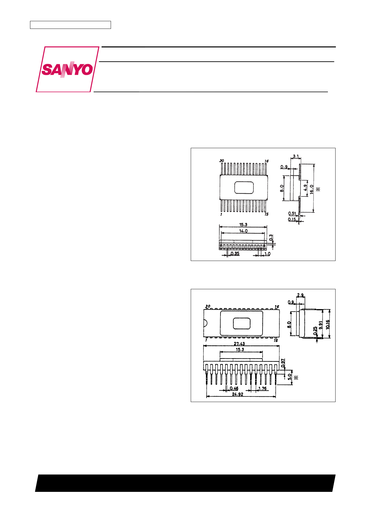
Package Dimensions
unit: mm
3212-MFC30S
[LC65E1104]
unit: mm
3215-DIC30S
SANYO: MFC30S
[LC65E1104]
SANYO: DIC30S
Note: These figures are provided for reference purposes and do not include
tolerance specifications. Official drawings are available on request
from your Sanyo representative.
SANYO Electric Co.,Ltd. Semiconductor Bussiness Headquarters
TOKYO OFFICE Tokyo Bldg., 1-10, 1 Chome, Ueno, Taito-ku, TOKYO, 110 JAPAN
73096HA (OT) No. 5221-1/19
1 page 
LC65E1104
Continued from preceding page.
Symbol
Pins I/O
Function
Option
PG0/AD4/A5
PG1/AD5/A6
PG2/AD6/A7
PG3/AD7/A8
4
AV+ 1
AV– 1
RES/VPP/OE
1
TEST/EPMOD
1
• I/O ports G0 to G3
Identical to PE0 to PE1*
Note: * No burst pulse output function is
provided.
I/O
• Each of these four pins has two functions as Identical to PE0 to
listed below.
PE1
PG0/AD4: AD converter input pin AD4
PG1/AD5: AD converter input pin AD5
PG2/AD6: AD converter input pin AD6
PG3/AD7: AD converter input pin AD7
— Reference voltage input pin for A/D
— conversion.
—
• System reset input
• Connect an external capacitor for power on
reset.
• Apply a low level for at least 4 clock cycles
for the power-on reset.
—
LSI test pin
Normally connected to VSS
—
At reset
Identical to PE0 to
PE1
—
—
—
PROM mode
Address inputs A5 to
A8
—
EPROM control signal
VPP/OE
EPROM control signal
EPMOD
Oscillator circuit option
Option
Circuit
Conditions and notes
1. External clock
Leave the OSC2 pin open.
2. 2-pin RC OSC
3. Ceramic oscillator
Predivider option
Option
1. No predivider (1/1)
2. 1/3 predivider
Circuit
Conditions and notes
• Applicable to all 3 oscillator options.
• The oscillator or external clock frequency must
not exceed 1444 kHz. (LC651104N,
LC651102N)
• The oscillator or external clock frequency must
not exceed 4330 kHz. (LC651104F,
LC651102F)
• The oscillator or external clock frequency must
not exceed 1040 kHz. (LC651104L,
LC651102L)
• Applicable to the external clock and ceramic
oscillator options.
• The oscillator or external clock frequency must
not exceed 4330 kHz.
3. 1/4 predivider
• Applicable to the external clock and ceramic
oscillator options.
• The oscillator or external clock frequency must
not exceed 4330 kHz.
Note: The oscillator and predivider options are summarized in the LC651104/1102 semiconductor news.
No. 5221-5/19
5 Page 
LC65E1104
Continued from preceding page.
Parameter
[Serial output]
Output delay time
[Pulse output]
Period
High-level pulse width
Low-level pulse width
[AD conversion characteristics]
Resolution
Absolute accuracy
Conversion time
Reference input voltage
Reference input current range
Analog input voltage range
Analog port input current
Symbol
Conditions
SO: Specified from the falling edge of SCK.
tCKO Nch OD only, external 1kΩ, external 50 pF, Fig. 6
tPCY
tPH
tPL
PE0: Fig. 7, tCYC = 4 × system clock period,
Nch OD only, external 1 kΩ, external 50 pF
TCAD
AV+
AV–
IRIF
VAIN
IAIN
VDD = 4.7 to 5.3 V
AV+ = VDD, AV– = VSS, VDD = 4.7 to 5.3 V
AD speed 1/1, at 26 × tCYC, VDD = 4.7 to 5.3 V
AD speed 1/2, at 51 × tCYC, VDD = 4.7 to 5.3 V
AV+: VDD = 4.7 to 5.3 V
AV–: VDD = 4.7 to 5.3 V
AV+, AV–: AV+ = VDD, VDD = 4.7 to 5.3 V, AV– = VSS
AD0 to AD7: VDD = 4.7 to 5.3 V
Port pins AD0 to AD7
Including output OFF leakage current. VAIN = VDD,
VDD= 4.7 to 5.3 V
Ratings
Unit
min typ max
0.6 µs
64 ×tCYC
32 × tCYC
± 10%
32 × tCYC
± 10%
µs
µs
µs
72 (tCYC
= 2.77 µs)
141 (tCYC
= 2.77 µs)
AV–
VSS
75
AV–
8
±1 ±2
312 (tCYC
= 12 µs)
612 (tCYC
= 12 µs)
VDD
AV+
150 300
AV+
bits
LSB
µs
V
µA
V
1
µA
Port pins AD0 to AD7
VAIN = VSS, VDD= 4.7 to 5.3 V
–1
[Watchdog timer]
Guaranteed constant*7
Clear time (discharge)
Clear time (charge)
Guaranteed constant*7
Clear time (discharge)
Clear time (charge)
Cw
Rw
RI
tWCT
tWCCY
Cw
Rw
RI
tWCT
tWCCY
WDR: VDD = 3 to 6 V
WDR: VDD = 3 to 6 V
WDR: VDD = 3 to 6 V
WDR: Fig. 8, VDD = 3 to 6 V
WDR: Fig. 8, VDD = 3 to 6 V
WDR: VDD = 4 to 6 V
WDR: VDD = 4 to 6 V
WDR: VDD = 4 to 6 V
WDR: Fig. 8, VDD = 4 to 6 V
WDR: Fig. 8, VDD = 4 to 6 V
0.1 ± 5%
680 ± 1%
100 ± 1%
100
36
0.047 ± 5%
680 ± 1%
100 ± 1%
40
18
µF
kΩ
Ω
µs
ms
µF
kΩ
Ω
µs
ms
Note: 1. The LC65E1104 will accept input voltages up to the generated oscillator amplitude if the oscillator circuit in figure 4 with circuit constants in the
guaranteed constants ranges is driven from within the IC.
2. Average over a 100 ms period
3. The operating supply voltage VDD must be held until standby mode is enterd after the execution of a HALT instruction. The PA3 pin must be free
from chattering during the HALT instruction cycle.
4. The OSC1 pin input circuit has Schmitt trigger characteristics when the 2-terminal RC oscillator option or the external clock oscillator option is
selected.
5. fCFOSC: oscillator frequency. The center frequency of a ceramic oscillator has a tolerance range of about 1% around the nominal value specified
by the manufacturer of the oscillator element. For details, refer to the specifications of the ceramic resonator.
6. TCYC = 4 × system clock period
7. If the LC65E1104 is used in an environment subject to condensation, leakage between PE1 and adjacent pins and leakage associated with
external RCA circuits require special attention.
No. 5221-11/19
11 Page | ||
| Páginas | Total 19 Páginas | |
| PDF Descargar | [ Datasheet LC65P1104.PDF ] | |
Hoja de datos destacado
| Número de pieza | Descripción | Fabricantes |
| LC65P1104 | On-Chip UVEPROM 4-Bit Single-Chip Microcontroller | Sanyo |
| LC65P1104 | One-Time Programmable 4-Bit Single-Chip Microcontroller | Sanyo |
| Número de pieza | Descripción | Fabricantes |
| SLA6805M | High Voltage 3 phase Motor Driver IC. |
Sanken |
| SDC1742 | 12- and 14-Bit Hybrid Synchro / Resolver-to-Digital Converters. |
Analog Devices |
|
DataSheet.es es una pagina web que funciona como un repositorio de manuales o hoja de datos de muchos de los productos más populares, |
| DataSheet.es | 2020 | Privacy Policy | Contacto | Buscar |