|
|
PDF K9S1208V0 Data sheet ( Hoja de datos )
| Número de pieza | K9S1208V0 | |
| Descripción | 64MB & 128MB SmartMediaTM Card | |
| Fabricantes | Samsung | |
| Logotipo |  |
|
Hay una vista previa y un enlace de descarga de K9S1208V0 (archivo pdf) en la parte inferior de esta página. Total 30 Páginas | ||
|
No Preview Available !
K9D1G08V0M/A-SSB0
K9S1208V0M/A-SSB0
SmartMediaTM
Document Title
64MB & 128MB SmartMediaTM Card
Revision History
Revision No History
Draft Date
0.0 Initial issue
Mar. 30th 2001
0.1 1. Changed DC characteristics
Apr. 7th 2001
Parameter
Min Typ
Max Unit
Operating Sequential Read
-
10
20->30
Current Program
-
10
20->30
mA
Erase
- 10 20->30
2. Added tDBSY parameter
3. Removed Copy-Back program command
4. Changed AC characteristics
Parameter
Symbol
ALE to RE Delay
( ID read )
tAR1
Min
100->10
Max
-
Unit
ns
Remark
Preliminary
0.2 1.Powerup sequence is added
Sep. 7th 2001
Recovery time of minimum 1µs is required before internal circuit gets
ready for any command sequences
~ 2.5V
~ 2.5V
VCC
High
WP
1µs
WE
2. AC parameter tCLR(CLE to RE Delay, min 50ns) is added.
3. Changed AC characteristics
(Before)
Parameter
Symbol
Min Max
ALE to RE Delay (ID read)
tAR1
100 -
ALE to RE Delay (Read
tAR2 100 -
RE Low to Status Output
tRSTO
- 35
CE Low to Status Output
tCSTO
- 45
RE access time(Read ID)
tREADID
-
35
Unit
ns
Note : For more detailed features and specifications including FAQ, please refer to Samsung’s Flash web site.
http://www.samsung.com/Products/Semiconductor/Flash/TechnicalInfo/datasheets.
The attached data sheets are prepared and approved by SAMSUNG Electronics. SAMSUNG Electronics CO., LTD. reserve the
right to change the specifications. SAMSUNG Electronics will evaluate and reply to your requests and questions about device. If you
have any questions, please contact the SAMSUNG branch office near your office.
1
1 page 
K9D1G08V0M/A-SSB0
K9S1208V0M/A-SSB0
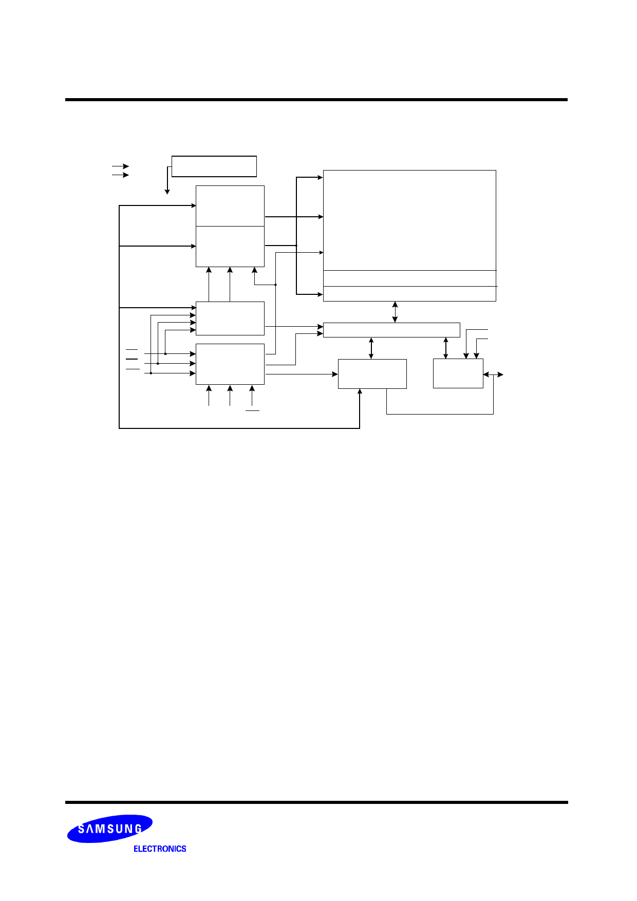
Figure 1. FUNCTIONAL BLOCK DIAGRAM
VCC
VSS
A25: K9S1208V0X
A26: K9D1G08V0X
A9 - A26
A0 - A7
X-Buffers
Latches
& Decoders
Y-Buffers
Latches
& Decoders
Command
A8
Command
Register
CE Control Logic
RE & High Voltage
WE Generator
CLE ALE WP
SmartMediaTM
K9S1208V0X : 512M + 16M Bit
K9D1G08V0X : 1,024M + 32M Bit
NAND Flash
ARRAY
K9S1208V0X : (512+16)Byte x 131,072
K9D1G08V0X : (512+16)Byte x 262,144
Page Register & S/A
Y-Gating
I/O Buffers & Latches
VCC
VSS
Global Buffers
Output
Driver
I/0 0
I/0 7
5
5 Page 
K9D1G08V0M/A-SSB0
K9S1208V0M/A-SSB0
SmartMediaTM
VALID BLOCK
Parameter
K9D1G08V0X
Valid Block Number
K9S1208V0X
Symbol
NVB
NVB
Min
8,052
4,026
Typ.
-
-
Max
8,192
4,096
Unit
Blocks
Blocks
1. The K9D1G08V0X, K9S1208V0X may include invalid blocks when first shipped. Additional invalid blocks may develop while being used. The num-
ber of valid blocks is presented with both cases of invalid blocks considered. Invalid blocks are defined as blocks that contain one or more bad bits. Do
not erase or program factory-market bad blocks. Refer to the attached technical notes for an appropriate management of invalid blocks.
2. Per the specification of the physical format version 1.2 by SSFDC forum, minimum 1,000 vaild blocks are guaranteed for each 16MB memory space.
AC TEST CONDITION
(TA=0 to 55°C, VCC=2.7V~3.6V unless otherwise noted)
Parameter
Input Pulse Levels
Input Rise and Fall Times
Input and Output Timing Levels
Output Load (3.0V +/-10%)
Output Load (3.3V +/-10%)
Value
0.4V to 2.4V
5ns
1.5V
1 TTL GATE and CL=50pF
1 TTL GATE and CL=100pF
CAPACITANCE(TA=25°C, VCC=3.3V, f=1.0MHz)
Item
Max
Symbol
Test Condition
Min
Unit
K9D1G08V0X K9S1208V0X
Input/Output Capacitance
CI/O
VIL=0V
-
20
10 pF
Input Capacitance
CIN VIN=0V
-
20
10 pF
NOTE : Capacitance is periodically sampled and not 100% tested.
MODE SELECTION
CLE
ALE
CE
WE
RE
WP
Mode
HLL
LHL
HX
Command Input
Read Mode
HX
Address Input(4clock)
HLL
LHL
HH
Command Input
Write Mode
HH
Address Input(4clock)
LLL
H H Data Input
L L LH
X sequential Read & Data Output
X X L X X X During Read(Busy)
X X X X X H During Program(Busy)
X X X X X H During Erase(Busy)
X X(1) X X X L Write Protect
X X H X X 0V/VCC(2) Stand-by
NOTE : 1. X can be VIL or VIH.
2. WP should be biased to CMOS high or CMOS low for standby.
11
11 Page | ||
| Páginas | Total 30 Páginas | |
| PDF Descargar | [ Datasheet K9S1208V0.PDF ] | |
Hoja de datos destacado
| Número de pieza | Descripción | Fabricantes |
| K9S1208V0 | 64MB & 128MB SmartMediaTM Card | Samsung |
| Número de pieza | Descripción | Fabricantes |
| SLA6805M | High Voltage 3 phase Motor Driver IC. |
Sanken |
| SDC1742 | 12- and 14-Bit Hybrid Synchro / Resolver-to-Digital Converters. |
Analog Devices |
|
DataSheet.es es una pagina web que funciona como un repositorio de manuales o hoja de datos de muchos de los productos más populares, |
| DataSheet.es | 2020 | Privacy Policy | Contacto | Buscar |
