|
|
|
PDF M52722SP Data sheet ( Hoja de datos )
| Número de pieza | M52722SP | |
| Descripción | 3-CHANNEL VIDEO PREAMPLIFIER PROVIDED WITH OSD MIX AND RETRACE LINE BLK FOR HIGH-RESOLUTION | |
| Fabricantes | Mitsubishi | |
| Logotipo | ||
Hay una vista previa y un enlace de descarga de M52722SP (archivo pdf) en la parte inferior de esta página. Total 17 Páginas | ||
|
No Preview Available !
MITSUBISHI ICs (Monitor)
M52722SP
3-CHANNEL VIDEO PREAMPLIFIER PROVIDED WITH OSD MIX
AND RETRACE LINE BLK FOR HIGH-RESOLUTION
DESCRIPTION
M52722SP is a video amplifier provided with OSD mixing function,
and a semiconductor IC having three channels of a built-in
wideband 180MHz amplifier.
Each channel has the functions of OSD blanking, OSD mixing,
retrace line blanking, wideband amplifier, main and sub contrast
control, and main brightness. Accordingly, it is structured to best fit
the OSD-provided high resolution display. .
FEATURES
• Frequency band : RGB...................................180MHz (at 3VP-P )
OSD....................................................50MHz
Input:
RGB..........................................0.7VP-P (Typ.)
OSD......................................more than 3VP-P
(positive polarity)
BLK (for OSD)......................more than 3VP-P
(positive polarity)
Retrace line BLK..................more than 3VP-P
(positive polarity)
Output:
RGB..........................................4.0VP-P (max.)
OSD..........................................4.0VP-P (max.)
• Each control of contrast and OSD adjustment includes a main
which allows 3 channels to be variable simultaneously, and a sub
which allows each channel to be variable independently. Each
control pin can be controlled within a range of 0 to 5V.
• A built-in feedback circuit inside IC provides a stable DC level at
IC output pins.
APPLICATION
CRT display
RECOMMENDED OPERATING CONDITION
Supply voltage range...........................................Vcc=11.5 to 12.5V
Rated supply voltage......................................................Vcc=12.0V
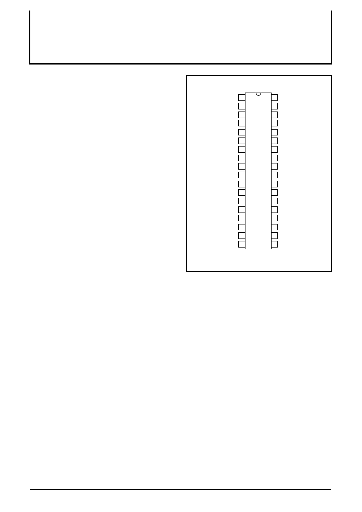
PIN CONFIGURATION (TOP VIEW)
BLK IN(for OSD) 1
VCC1 (B) 2
INPUT (B) 3
SUB CONTRAST (B) 4
OSD IN (B) 5
GND 1 (B) 6
VCC1 (G) 7
INPUT (G) 8
SUB CONTRAST (G) 9
OSD IN (G) 10
GND 1 (G) 11
VCC1 (R) 12
INPUT (R) 13
SUB CONTRAST (R) 14
OSD IN (R) 15
GND 1 (R) 16
MAIN CONTRAST 17
CP IN 18
36 MAIN OSD ADJUST
35 OUTPUT (B)
34 VCC2 (B)
33 HOLD (B)
32 SUB OSD ADJUST (B)
31 GND2 (B)
30 OUTPUT (G)
29 VCC2 (G)
28 HOLD (G)
27 SUB OSD ADJUST (G)
26 GND2 (G)
25 OUTPUT (R)
24 VCC2 (R)
23 HOLD (R)
22 SUB OSD ADJUST (R)
21 GND2 (R)
20 BLK IN (for retrace)
19 BRIGHTNESS
Outline 36P4E
1
1 page 
MITSUBISHI ICs (Monitor)
M52722SP
3-CHANNEL VIDEO PREAMPLIFIER PROVIDED WITH OSD MIX
AND RETRACE LINE BLK FOR HIGH-RESOLUTION
ELECTRICAL CHARACTERISTICS (cont.)
Symbol
SOaj1
SOaj2
HBLK
HVth
Parameter
SUB OSD adjustment control
characteristics (at typ.)
SUB OSD adjustment control
characteristics (at min.)
Retrace line BLK characteris-
tics
Retrace line BLK input
threshold value
Test
point
T.P35
T.P30
T.P25
T.P35
T.P30
T.P25
T.P35
T.P30
T.P25
T.P35
T.P30
T.P25
SW3
R-ch
a
_
a
_
a
_
a
_
Input
SW8 SW13
G-ch B-ch
aa
__
aa
__
aa
__
aa
__
External power supply(v) Pulse input
Limits
V4
V17
V19
V32
V36
SW18
SW1
5,10,15
SW20
Min.
Typ. Max.
5
5
2
2
5
bb
SG4 SG6
a
_
1.6 2.2 2.6
5
5
2
0
5
bb
SG4 SG6
a
_
-
0 0.5
55
20
0
a
_
a
_
b
SG7
-
0.2 0.5
55
20
0
a
_
a
_
b
SG7
0.5
1.5
2.5
Unit
VP-P
VP-P
VDC
VDC
ELECTRICAL CHARACTERISTICS TEST METHOD
Note: SW/NO of signal input pin and SW/NO of pulse input pin,
which have already been described in the electrical characteristics
table, are omitted, and SW/NO of external power supply will only be
described as follows:
Sub-OSD adjustment voltages, V32, V27 and V22, which are
always set to the identical value, are represented by V32 in the
electrical characteristics table. In addition, sub-contrast voltages,
V4, V9 and V14, which are also set to the identical value, are
represented by V4 in the electrical characteristics table.
Icc circuit current
Conditions shall be as specified in the electrical characteristics
table, and take measurements with ammeter A when SWA is turned
to the b side.
Vomax output dynamic range
Follow the following procedure to set V19.
1. Input SG5 to pin 13 (pin 8 or pin 3 ), gradually reduce V19, and
read the lower part voltage when the lower part of input
waveform of T.P25 (T.P30 or T.P35) is distorted to let the reading
be VOLR (VOLG or VOLB).
2. Then, gradually raise V19, and read the upper part voltage when
the upper part of output waveform of T.P25 (T.P30 or T.P35) is
distorted to let the reading be VOHR (VOHG or VOHB).
3. Vomax is found by:
Vomax=VOHR(VOHG, VOHB)-VOLR(VOLG, VOLB)
(V)
Vimax maximum allowable input
Change V17 to 2.5V, gradually increase input signal amplitude from
700m VP-P, and read input signal amplitude when output signal
starts to be distorted.
Gv and ∆Gv maximum gain and relative maximum gain
1. Input SG5 to pin 13 (pin 8 or pin 3 ), and read the output
amplitude of T.P25 (T.P30 or T.P35) at this time to let the reading
be VOR1 (VOG1 or VOB1).
2. Maximum gain Gv is found by:
GV=20LOG
VOR1(VOG1, VOB1) [VP-P]
0.7 [VP-P]
3. Relative maximum gain ∆G is found by
∆GV=VOR1/VOG1, VOG1/VOB1, VOB1/VOR1
through respective calculation.
VCR1 contrast control characteristics and
∆VCR1 relative contrast control characteristics (at typ.)
1. Follow the electrical characteristics table except changing V17 to
4V.
2. Read the output amplitude of T.P25 (T.P30 or T.P35) at this time,
and let the reading be VOR2 (VOG2 or VOB2).
3. Contrast control characteristics VCR1 and relative contrast
control characteristics ∆VCR1 is found by
VCR1=20LOG
VOR2(VOG2, VOB2) [VP-P]
0.7 [VP-P]
∆VCR1=VOR1/VOG1, VOG1/VOB1, VOB1/VOR1
5.0
0.0
T.P25 output waveform (T.P30 and T.P35 are also the same)
through respective calculation.
VCR2 contrast control characteristics and
∆VCR2 relative contrast control characteristics (at min.)
1. Follow the electrical characteristics table except changing V17 to
1.0V.
2. Read the output amplitude of T.P25 (T.P30 or T.P35) at this time
to let the reading be VOR3 (VOG3 or VOB3). This value represents
VCR2.
3. Relative contrast control characteristics ∆VCR2 is found by:
VOR2 = VOR3/ VOG3,VOG3/ VOB3/ ,VOB3/VOR3
5
5 Page 
MITSUBISHI ICs (Monitor)
M52722SP
3-CHANNEL VIDEO PREAMPLIFIER PROVIDED WITH OSD MIX
AND RETRACE LINE BLK FOR HIGH-RESOLUTION
TYPICAL CHARACTERISTICS
THERMAL DERATING (MAXIMUM RATING)
2400
2016
2000
1600
1200
800
400
0
-20 0
When mounted with
standard substrate
25 50 75 85 100 125 150
OPERATING TEMPERATURE Ta (˚C)
11
11 Page | ||
| Páginas | Total 17 Páginas | |
| PDF Descargar | [ Datasheet M52722SP.PDF ] | |
Hoja de datos destacado
| Número de pieza | Descripción | Fabricantes |
| M52722SP | 3-CHANNEL VIDEO PREAMPLIFIER PROVIDED WITH OSD MIX AND RETRACE LINE BLK FOR HIGH-RESOLUTION | Mitsubishi |
| M52722SP | 3-CHANNEL VIDEO PREAMPLIFIER PROVIDED WITH OSD MIX AND RETRACE LINE BLK FOR HIGH-RESOLUTION | Mitsubishi |
| Número de pieza | Descripción | Fabricantes |
| SLA6805M | High Voltage 3 phase Motor Driver IC. |
Sanken |
| SDC1742 | 12- and 14-Bit Hybrid Synchro / Resolver-to-Digital Converters. |
Analog Devices |
|
DataSheet.es es una pagina web que funciona como un repositorio de manuales o hoja de datos de muchos de los productos más populares, |
| DataSheet.es | 2020 | Privacy Policy | Contacto | Buscar |