|
|
|
PDF M52746SP Data sheet ( Hoja de datos )
| Número de pieza | M52746SP | |
| Descripción | BUS CONTROLLED 3CH VIDEO PRE-AMP FOR CRT DISPLAY MONITOR | |
| Fabricantes | Mitsubishi | |
| Logotipo | ||
Hay una vista previa y un enlace de descarga de M52746SP (archivo pdf) en la parte inferior de esta página. Total 25 Páginas | ||
|
No Preview Available !
MITSUBISHI< LINEAR IC >
M52746SP
BUS CONTROLLED 3CH VIDEO PRE-AMP FOR CRT DISPLAY MONITOR
DISCRIPTION
M52746SP is Semiconductor Integrated Circuit
for CRT Display Monitor.
It includes OSD Blanking,OSD Mixing,Retrace
Blanking,Wide Band Amplifre,Brightness Control.
Main/Sub Contrast and OSD AdjustFunction can be
controlled by I2C Bus.
FEATURES
Frequency Band Width: RGB 200 MHz (at -3dB)
OSD 80 MHz
Input : RGB
0.7 Vp-p (Typ)
OSD light
4 Vp-p minimum (positive)
OSD harf
2.5Vp-p minimum (positive)
3.0Vp-p maximum (positive)
BLK(for OSD) 3 Vp-p minimum (positive)
Retrace BLK 3 Vp-p minimum (positive)
Output : RGB
5.5 Vp-p (maximum)
OSD
5 Vp-p (maximum)
PIN CONFIGURATION
Brightness
OSD IN (R)
OSD IN (B)
OSD IN (G)
OSD BLK IN
INPUT (R)
VCC 12V
NC
INPUT (B)
GND
INPUT (G)
VCC 12V
INPUT(SOG)
SOG Sep OUT
GND
Clamp Pulse IN
1
2
3
4
5
6
7
8
9
10
11
12
13
14
15
16
32 VCC 12V (R)
31 OUTPUT(R)
30 GND(R)
29 VCC 12V (B)
28 OUTPUT(B)
27 GND(B)
26 GND
25 VCC 12V (G)
24 OUTPUT(G)
23 GND(G)
22 Retrace BLK IN
21 SDA
20 SCL
19 GND
18 ABL IN
17 VCC 5V
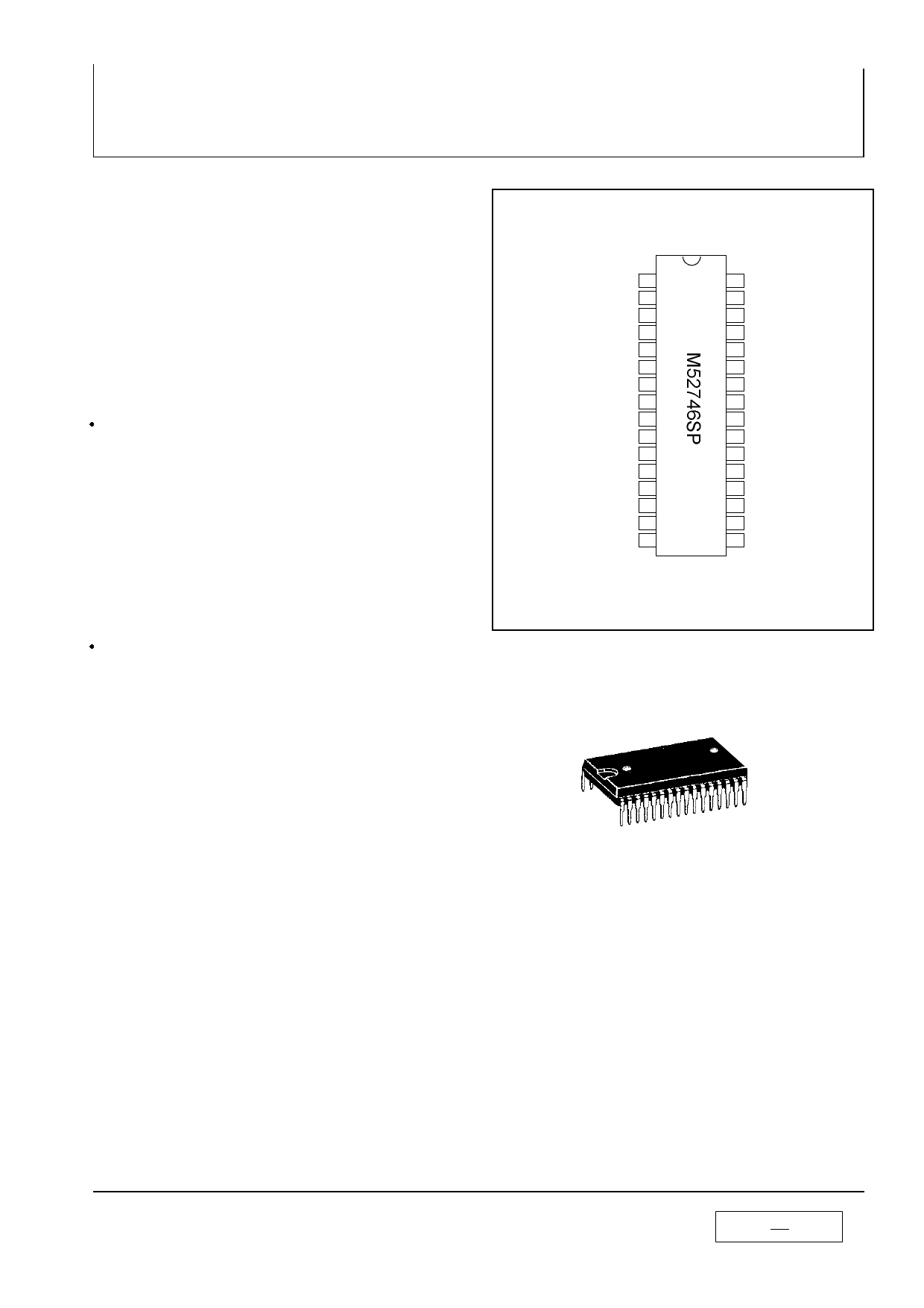
Outside Package: 32P4B
Main Contrast and Sub Contrast can be controlled by I2C
Bus.
STRUCTURE
Bipola Silicon Monolisic IC
APPLICATION
CRT Display Monitor
RECOMMENDED OPERATING CONDITIONS
Supply Voltage Range 11.5V~12.5V(V7,V12,V25,V29,V32)
4.5V~4.4V(V17)
Rated Supply Voltage 12.0V(V7,V12,V25,V29,V32)
5.0V(V17)
MAJOR SPECIFICATION
Bus Controlled 3ch Video Pre-Amp with OSD Mixing Function
32 pin plastic SDIP
MITSUBISHI
1 25
1 page 
MITSUBISHI< LINEAR IC >
M52746SP
BUS CONTROLLED 3CH VIDEO PRE-AMP FOR CRT DISPLAY MONITOR
2
I C BUS CONTROL SECTION
SDA,SCL CHARACTERISTICS
parameter
symbol
MIN
MAX
unit
min. input LOW voltage.
VIL -0.5 1.5 V
max. input HIGH voltage.
VIH 3.0 5.5 V
SCL clock frequency.
fSCL 0 100 KHz
Time the bus must be free before a new transmission can start. tBUF 4.7 - us
Hold time start condition.After this period the first clock pulse
is generated.
tHD:STA
4.0
- us
The LOW period of the clock.
The HIGH period of the clock.
Srt up time for start condition. (Only relevant for a repeated
start condition.)
Hold time DATA.
Set-up time DATA.
Rise time of both SDA and SCL lines.
Fall time of both SDA and SCL lines.
Set-up time for stop condition.
tLOW 4.7 - us
tHIGH 4.0 - us
tSU:STA
4.7
- us
tHD:DAT
0
- us
tSU:DAT
250
- ns
tR
-
1000
ns
tF
tSU:STO
-
4.0
300 ns
- us
VIL
SDA
VIH
tR, tF
tBUF
VIL
SCL
VIH
tHD:STA
S
tSU:DAT
tHD:DAT
tLOW
tHIGH
tSU:STA
S
tSU:ST
O
PS
MITSUBISHI
5 25
5 Page 
MITSUBISHI< LINEAR IC >
Note1)
M52746SP
BUS CONTROLLED 3CH VIDEO PRE-AMP FOR CRT DISPLAY MONITOR
Measuring conditions are as listed in supplementary Table. Measured with a current
meter at test point IA.
Note2) Measuring conditions are as listed in supplementary Table. Measured with a current
meter at test point IB.
Note3)
Decrease V1 gradually, and measure the voltage when the bottom of waveform output is
distorted. The voltage is called VCL.
Next, increase V1 gradually, and measure the voltage when the top of waveform output is
distorted. The voltage is called VOH.
Voltagr Vomax is calculated by the equation below:
Vomax = VOH - VOL
(V)
VOH
5.0
Waveform output
Note4)
VOL
0.0
Increase the input signal(SG2) amplitude gradually, starting from 700mVp-p. Measure the
amplitude of the input signal when the output signal starts becoming distorted.
Note5)
Input SG1, and read the amplitude output at OUT(24,28,31). The amplitude is called
VOUT(24,28,31).Maximum gain GV is calculated by the equation below:
GV=20 LOG
VOUT
0.7
(dB)
Note6) Relative maximum gain GV is calculated by the equation below:
GV=VOUT(24)/VOUT(18), VOUT(28)/VOUT(31), VOUT(31)/VOUT(24)
Note7)
Measuring the amplitude output at OUT(24,28,31). The measured value is called
VOUT(24,28,31).
Main contrast conrol characteristics VC1 is calculated by the equation below:
VOUT
VC1=20 LOG
0.7
(dB)
Note8) Relative characteristics VC1 is calculated by the equation below:
VC1=VOUT(24)/VOUT(28) , VOUT(28)/VOUT(31) , VOUT(31)/VOUT(24)
Note9) Measuring condition and procedure are the same as described in Note7.
Note10) Measuring condition and procedure are the same as described in Note8.
Note11) Measuring condition and procedure are the same as described in Note7.
Note12) Measuring condition and procedure are the same as described in Note8.
MITSUBISHI
11 25
11 Page | ||
| Páginas | Total 25 Páginas | |
| PDF Descargar | [ Datasheet M52746SP.PDF ] | |
Hoja de datos destacado
| Número de pieza | Descripción | Fabricantes |
| M52746SP | BUS CONTROLLED 3CH VIDEO PRE-AMP FOR CRT DISPLAY MONITOR | Mitsubishi |
| M52746SP | BUS CONTROLLED 3CH VIDEO PRE-AMP FOR CRT DISPLAY MONITOR | Mitsubishi |
| Número de pieza | Descripción | Fabricantes |
| SLA6805M | High Voltage 3 phase Motor Driver IC. |
Sanken |
| SDC1742 | 12- and 14-Bit Hybrid Synchro / Resolver-to-Digital Converters. |
Analog Devices |
|
DataSheet.es es una pagina web que funciona como un repositorio de manuales o hoja de datos de muchos de los productos más populares, |
| DataSheet.es | 2020 | Privacy Policy | Contacto | Buscar |