|
|
|
PDF M52338FP Data sheet ( Hoja de datos )
| Número de pieza | M52338FP | |
| Descripción | INTERFACE IC FOR ACTIVE MATRIX LIQUID CRYSTAL PANEL | |
| Fabricantes | Mitsubishi | |
| Logotipo | ||
Hay una vista previa y un enlace de descarga de M52338FP (archivo pdf) en la parte inferior de esta página. Total 12 Páginas | ||
|
No Preview Available !
MITSUBISHI ICs (TV)
M52338FP
INTERFACE IC FOR ACTIVE MATRIX LIQUID CRYSTAL PANEL
DESCRIPTION
The M52338FP is a semiconductor integrated circuit containing an
interface circuit which is necessary to drive an active matrix liquid
crystal panel.
FEATURES
• γ correction circuit is built in to correct non-linearity of luminance
characteristics caused by applied voltage which is peculiar to a
liquid crystal panel.
• By combining with Mitsubishi video/chroma signal processing
ICs, M52042FP (NTSC) and M52045FP (PAL), low cost and
optimal system configuration is possible.
APPLICATION
Active matrix liquid crystal color television
RECOMMENDED OPERATING CONDITION
Supply voltage
GND=0V,VCC1=VCC2
VCC1
VCC2
VEE
Operating Recommended
supply voltage supply voltage
4.0 to 5.5V
4.5V
-7.0 to 8.5V
-7.5V
PIN CONFIGURATION (TOP VIEW)
MAIN IN R 1
CLAMP R 2
MAIN IN G 3
CLAMP G 4
MAIN IN B 5
CLAMP B 6
MAIN/EXT SW 7
HD IN 8
CP CONT. 9
VCC2 10
VEE 11
FRP2 IN 12
COMMON GAIN CONT. 13
COMMON OUT 14
BIAS CONT. 15
GND 16
32 VCC1
31 EXT IN R
30 SUB CONTRAST B
29 EXT IN G
28 SUB CONTRAST R
27 EXT IN R
26 γ2
25 γ1
24 CONTRAST
23 BRIGHT
22 FRP1 IN
21 R OUT
20 SUB BIAS R
19 G OUT
18 SUB BIAS B
17 B OUT
Outline 32P2U-B
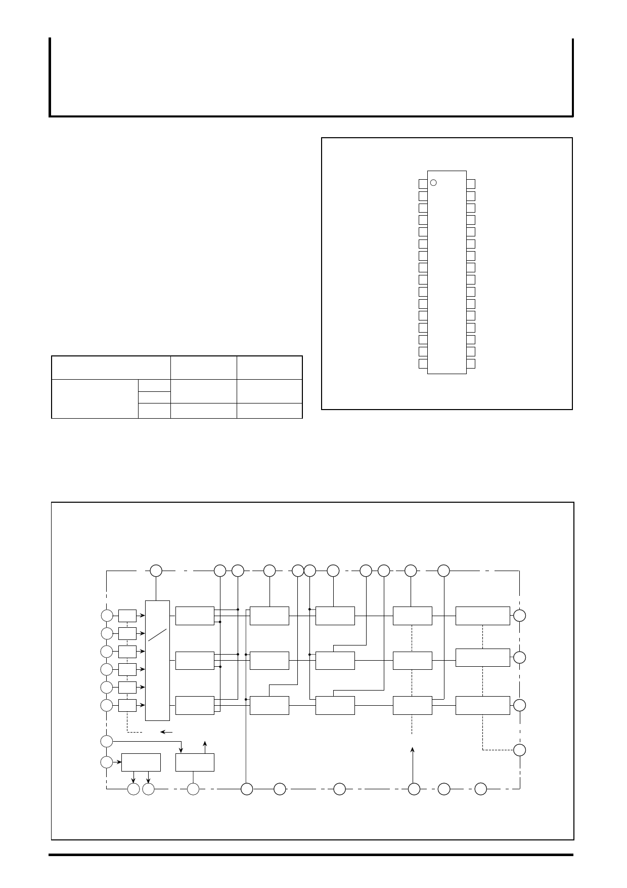
BLOCK DIAGRAM
SW
7
γ1 γ2
25 26
SUB
SUB
SUB
CONTRAST CONTRAST
CLAMP G
BIAS
R
B BRIGHT CLAMP R
CLAMP B R
28
30 23
2
46
20
SUB
BIAS
B
18
MAIN IN R 1 CP
MAIN IN G 3 CP
MAIN IN B 5 CP
EXT IN R 27 CP
EXT IN G 29 CP
EXT IN B 31 CP
MAIN
EXT
SW
γ-AMP
γ-AMP
γ-AMP
CONTRAST
CONTRAST
CONTRAST
HO IN 8
FRP2 IN 12
CP
COMMON
INV
CP
CLAMP
13 14
COMMON GAIN COMMON
CONT.
OUT
9
CP
CONT.
24 32
CONTRAST VCC1
BRIGHT
CLAMP
BRIGHT
CLAMP
BRIGHT
CLAMP
16
GND
SUB BIAS
SUB BIAS
DRIVE BUFFER 21 R OUT
PEAK LIMITER
DRIVE BUFFER
PEAK LIMITER
19 G OUT
SUB BIAS
FRP1
DRIVE BUFFER 17 B OUT
PEAK LIMITER
BIAS
15 CONT.
22
FRP1 IN
10
VCC2
11
VEE
1 page 
MITSUBISHI ICs (TV)
M52338FP
INTERFACE IC FOR ACTIVE MATRIX LIQUID CRYSTAL PANEL
ELECTRICAL CHARACTERISTICS TEST METHOD
ICC1,ICC2
Circuit current 1, 2
Measure quiescent current flowing into pins 1 and 10 .
COmin1,COmax1
Common output 1
Input FRP2 and measure the output amplitude when voltage at
pin 13 is changed to GND, and 4.5V.
COminT1,COmaxT1 Common center voltage level 1
Input FRP2 and measure the center voltage level of output
waveform when voltage at pin 13 is changed to GND, and 4.5V.
cothH1,cothL1 Common through rate 1
Input FRP2 and measure through rates at rising point and
falling point of the output waveform when voltage at pin 13 is
connect-ed to GND.
MA1 Maximum input level A
Connect pin 22 to 4.5V and measure the non-inverted output
amplitude between pedestal level and white level at pins 17 , 19 ,
and 21 when signal Y (1.5VP-P) is input. Also, measure in the
same way as above when pin 7 is connected to GND and the
mode is changed to EXT.
MOA1 Offset among channels at maximum input level A
Based on the results of maximum input level A, calculate the
difference in amplitude level among channels.
MB1 Maximum input level B
Connect pin 22 to GND and measure the inverted output
amplitude between pedestal level and white level at pins 17 , 19 ,
and 21 when signal Y (1.5VP-P) is input. Also, measure in the
same way as above when pin 7 is connected to GND and the
mode is changed to EXT.
MOB1 Offset among channels at maximum input level B
Based on the results of the maximum input level B, calculate
the difference in amplitude level among channels.
M1 Maximum input level difference
Calculate difference in output amplitude between maximum
input level A and level B of each channel.
P11 Pedestal voltage level 1
In inputting signal Y, measure output voltage at pins 17 , 19 ,
and 21 when pin 22 is 4.5V and pin 24 is grounded. Also,
measure in the same way as above when pin 7 is connected
to GND and the mode is changed to EXT.
PO11 Offset among channels at pedestal voltage level 1
Based on the results of pedestal voltage level 1, calculate
offset among channels.
PO21 Pedestal voltage level 2
In inputting signal Y, measure output voltage at pins 17 , 19 ,
and 21 when voltage at pins 22 and 24 are connected to GND.
Also, measure in the same way as above when pin 7 is
connected to GND and the mode is changed to EXT.
PO21 Offset among channels at pedestal voltage level 2
Based on the results of pedestal voltage level 2, calculate offset
among channels.
S1 Center output voltage level
Measure the center voltage level based on pedestal voltage
levels 1 and 2 of each channel.
M=(pedestal voltage level 1 - pedestal voltage level 2) /2
SO1
Offset among channels at center
output voltage level
Based on the result of center output voltage level, measure
offset among channels.
A1 Output amplitude A
In inputting signal Y, measure non-inverted output amplitude
between pedestal level and white level at pins 17 , 19 ,and 201
when pin 22 is 4.5V and voltage at pin 24 is 1.5V. Also, measure
in the same way as above when pin 7 is connected to GND
and the mode is changed to EXT.
OA1
Offset among channels at output amplitude A
Based on the results of output amplitude A, calculate the
difference in output amplitude among channels.
B1 Output amplitude B
In inputting signal Y, measure non-inverted output amplitude
between pedestal level and white level at pins 17 , 19 , and 210
when voltage at pin 22 is grounded and voltage at pin 24 is 1.5V.
Also, measure in the same way as above, when pin 7 is
connected to GND and the mode is changed to EXT.
OB1
Offset among channels at output amplitude B
Based on the results of output amplitude B, calculate the
difference in output amplitude among channels.
L1 Linearity
Measure the difference in inverted/inverted output amplitude of
the output waveform found as the results of output amplitude A
and B. Also, measure in the same way as above, when pin 7 is
connected to GND and the mode is changed to EXT.
W11
White balance 1
In inputting signal Y, measure white peak level of each channel
when voltage at pin 22 and 24 are 4.5V (in the state that peak
limiter work). Also, measure in the same way as above when
pin 7 is connected to 4.5V and the mode is changed to EXT.
WO11 Offset among channels at white balance 1
Based on the results of white balance 1, measure offset among
channels.
W21
White balance 2
In inputting signal Y, measure white peak level of each channel
when pin 22 is grounded and voltage at pin 24 is 4.5V (in the
state peak limiter works). Also, measure in the same way as
above when pin 7 is connected to GND and the mode is
changed to EXT.
5 Page 
MITSUBISHI ICs (TV)
M52338FP
INTERFACE IC FOR ACTIVE MATRIX LIQUID CRYSTAL PANEL
DESCRIPTION OF PIN
Pin No.
Name
MAIN IN R
1 (Main signal input Rch)
Peripheral circuit pins
Vcc1
135
MAIN IN G
3 (Main signal input Gch)
5
MAIN IN B
(Main signal input Bch)
GND
CP
2
CLAMP R
(Clamped capacitance R)
VCC1
24 6
Pin No.
10
Name
VCC2
(Power supply)
V11
EE
(Grounded or - Power supply)
Peripheral circuit pins
VCC1
VCC2
12
FRP2
12 (FRP2 input)
4 CLAMP G
(Clamped capacitance G)
5k
6
CLAMP B
(Clamped capacitance B)
GND
VCC1
SW
7 (MAIN/EXT SW)
CP
GND
VEE
VCC1
13
COMMON
13 GAIN CONT.
(Commom gain control)
GND
GND
VCC1 8
HD IN
8 (HD pulse input)
GND
9
VCC1
CP CONT.
9 (Clamp pulse control)
GND
7
VCC2
14 COMMON OUT
(Commom output)
V
VEE
15
VCC1
BIAS CONT.
15 (Bias control)
16 GND
(Grounding)
GND
14
11 Page | ||
| Páginas | Total 12 Páginas | |
| PDF Descargar | [ Datasheet M52338FP.PDF ] | |
Hoja de datos destacado
| Número de pieza | Descripción | Fabricantes |
| M52338FP | INTERFACE IC FOR ACTIVE MATRIX LIQUID CRYSTAL PANEL | Mitsubishi |
| M52338FP | INTERFACE IC FOR ACTIVE MATRIX LIQUID CRYSTAL PANEL | Mitsubishi |
| Número de pieza | Descripción | Fabricantes |
| SLA6805M | High Voltage 3 phase Motor Driver IC. |
Sanken |
| SDC1742 | 12- and 14-Bit Hybrid Synchro / Resolver-to-Digital Converters. |
Analog Devices |
|
DataSheet.es es una pagina web que funciona como un repositorio de manuales o hoja de datos de muchos de los productos más populares, |
| DataSheet.es | 2020 | Privacy Policy | Contacto | Buscar |