|
|
|
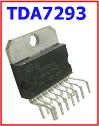
PDF TDA7293 Data sheet ( Hoja de datos )
| Número de pieza | TDA7293 | |
| Descripción | DMOS audio amplifier | |
| Fabricantes | ST Microelectronics | |
| Logotipo | ||
 1. Audio Amplifer - ST Hay una vista previa y un enlace de descarga de TDA7293 (archivo pdf) en la parte inferior de esta página. Total 21 Páginas | ||
|
No Preview Available !
TDA7293
120-volt, 100-watt, DMOS audio amplifier
with mute and standby
Features
Multipower BCD technology
Very high operating voltage range (±50 V)
DMOS power stage
High output power (100 W into 8 Ω
@ THD =10%, with VS = ±40 V)
Muting and stand-by functions
No switch on/off noise
Very low distortion
Very low noise
Short-circuit protected (with no input signal
applied)
Thermal shutdown
Clip detector
Modularity (several devices can easily be
connected in parallel to drive very low
impedances)
Description
The TDA7293 is a monolithic integrated circuit in
Multiwatt15 package, intended for use as audio
Multiwatt15V
Multiwatt15H
class AB amplifier in Hi-Fi field applications, such
as home stereo, self powered loudspeakers and
Topclass TV. Thanks to the wide voltage range
and to the high output current capability it is able
to supply the highest power into both 4-Ω and 8-Ω
loads.
The built-in muting function with turn-on delay
simplifies the remote operation avoiding on-off
switching noises.
Parallel mode is possible by connecting several
devices and using pin11. High output power can
be delivered to very low impedance loads, so
optimizing the thermal dissipation of the system
Table 1. Device summary
Order code
Package
TDA7293V
Multiwatt15V
TDA7293HS
Multiwatt15H
Figure 1.
TDA7293 block diagram
C7 100nF
+Vs C6 1000µF
VMUTE
VSTBY
R3 22K
C2
22µF
R2
680Ω
IN- 2
C1 470nF
IN+ 3
R1 22K
SGND
(**)
4
+Vs
-
+
R5 10K
R4 22K
C3 10µF
MUTE 10
STBY 9
MUTE
STBY
C4 10µF
1
STBY-GND
(*) see Application note
(**) for SLAVE function
BUFFER DRIVER
7 11
+PWVs
13
14 OUT
THERMAL
SHUTDOWN
S/C
PROTECTION
BOOT
12 LOADER
C5
22µF
(*)
6
BOOTSTRAP
5
VCLIP
CLIP DET
8
-Vs
C9 100nF
15
-PWVs
C8 1000µF
-Vs
D97AU805A
September 2010
Doc ID 6744 Rev 8
1/21
www.st.com
21
1 page 
TDA7293
Electrical specifications
2.3 Electrical characteristics
The specifications given here were obtained with the conditions VS = ±40 V, RL = 8 Ω,
Rg = 50 Ω, Tamb = 25 °C, f = 1 kHz unless otherwise specified.
Table 4.
Symbol
.
Electrical characteristics
Parameter
Test conditions
Min Typ Max Unit
VS Supply range
Iq Quiescent current
Ib Input bias current
VOS Input offset voltage
IOS Input offset current
PO Continuous output power
d Total harmonic distortion (1)
ISC
SR
GV
GV
eN
Ri
SVR
Current limiter threshold
Slew rate
Open loop voltage gain
Closed loop voltage gain (2)
Total input noise
Input resistance
Supply voltage rejection
TS Thermal protection
Standby function (ref. to to pin 1)
VST on
Standby on threshold
VST off
Standby off threshold
ATTst-by Standby attenuation
Iq st-by
Quiescent current @ standby
Mute function (ref. to pin 1)
VMon
VMoff
ATTmute
Mute on threshold
Mute off threshold
Mute attenuatIon
-
-
-
-
-
d = 1%, RL = 4 Ω,
VS = ±29 V
d = 10%, RL = 4Ω,
VS = ±29 V
PO = 5 W, f = 1 kHz
PO = 0.1 to 50 W,
f = 20 Hz to 15 kHz
VS ≤ ±40 V
-
-
-
A = curve
f = 20 Hz to 20 kHz
-
f = 100 Hz,
Vripple = 0.5 V RMS
Device mutes
Device shuts down
±12 -
±50 V
- 50 100 mA
-
0.3 1
µA
-10 -
10 mV
- - 0.2 µA
75
80
80
-
W
90
100
100
-
W
- 0.005 - %
- - 0.1 %
- 6.5
5 10
- 80
29 30
-1
-3
100 -
-
-
-
31
-
10
-
A
V/µs
dB
dB
µV
µV
kΩ
- 75 - dB
- 150 - °C
- 160 - °C
- - - 1.5 V
- 3.5 - - V
-
70 90 -
dB
-
-
0.5 1
mA
- - - 1.5 V
- 3.5 - - V
-
60 80 -
dB
Doc ID 6744 Rev 8
5/21
5 Page 
TDA7293
Applications information
4.2 High efficiency
Constraints of implementing high power solutions are the power dissipation and the size of
the power supply. These are both due to the low efficiency of conventional AB class
amplifier approaches.
The circuit below in Figure 8 is a high efficiency amplifier which can be adopted for both hi-fi
and car-radio applications. The TDA7293 is a monolithic MOS power amplifier which can be
operated with a 100-V supply (120 V with no signal applied) while delivering output currents
up to ±6.5 A. This allows the use of this device as a very high-power amplifier (up to 180 W
peak power with THD = 10% and RL = 4 Ω); the only drawback is the power dissipation,
hardly manageable in the above power range.
The typical junction-to-case thermal resistance of the TDA7293 is 1 °C/W (max = 1.5 °C/W).
In worst case conditions, to avoid the chip temperature exceeding 150 °C the thermal
resistance of the heatsink must be 0.038 °C/W (at a maximum ambient temperature of
50 °C).
As the above value is pratically unreachable, a high efficiency system is needed in those
cases where the continuous average output power is higher than 50 to 60 W.
The TDA7293 was designed to work also in a higher efficiency way. For this reason there
are four power supply pins: two intended for the signal part and two for the power part. T1
and T2 are two power transistors that only operate when the output power reaches a certain
threshold (for example, 20 W).
If the output power increases, these transistors are switched on during the portion of the
signal where more output voltage swing is needed, thus "bootstrapping" the power supply
pins (13 and 15). The current generators formed by T4, T7, zener diodes Z1, Z2 and
resistors R7, R8 define the minimum drop across the power MOS transistors of the
TDA7293. L1, L2, L3 and the snubbers C9, R1 and C10, R2 stabilize the loops formed by
the "bootstrap" circuits and the output stage of the TDA7293.
By considering again a maximum average output power (music signal) of 20 W, in case of
the high efficiency application, the thermal resistance value needed from the heatsink is
2.2 °C/W (with VS = ±50 V and RL = 8 Ω). All components (TDA7293 and power transistors
T1 and T2) can be placed on a 1.5 °C/W heatsink, with the power darlingtons electrically
insulated from the heatsink.
Since the total power dissipation is less than that of a usual class AB amplifier, additional
cost savings can be obtained while optimizing the power supply, even with a large heatsink.
4.3 Bridge application
Another application suggestion is the bridge configuration, where two TDA7293 are used.
In this application, the value of the load must not be lower than 8 Ω for dissipation and
current capability reasons.
A suitable field of application includes hi-fi/TV subwoofer realizations. The main advantages
offered by this solution are:
z High power performance with limited supply voltage level.
z Considerably higher output power even with high load values, such as 16 Ω.
With RL = 8 Ω and VS = ±25 V, the maximum output power obtainable is 150 W, whilst with
RL = 16 Ω and VS = ±40 V, the maximum Pout is 200 W.
Doc ID 6744 Rev 8
11/21
11 Page | ||

| Páginas | Total 21 Páginas | |
| PDF Descargar | [ Datasheet TDA7293.PDF ] | |
Hoja de datos destacado
| Número de pieza | Descripción | Fabricantes |
| TDA7292 | 40 + 40W Stereo Amplifier | STMicroelectronics |
| TDA7293 | DMOS audio amplifier | ST Microelectronics |
| TDA7293V | 120V - 100W DMOS AUDIO AMPLIFIER WITH MUTE/ST-BY | ST Microelectronics |
| TDA7294 | 100V - 100W DMOS AUDIO AMPLIFIER WITH MUTE/ST-BY | ST Microelectronics |
| Número de pieza | Descripción | Fabricantes |
| SLA6805M | High Voltage 3 phase Motor Driver IC. |
Sanken |
| SDC1742 | 12- and 14-Bit Hybrid Synchro / Resolver-to-Digital Converters. |
Analog Devices |
|
DataSheet.es es una pagina web que funciona como un repositorio de manuales o hoja de datos de muchos de los productos más populares, |
| DataSheet.es | 2020 | Privacy Policy | Contacto | Buscar |