|
|
|
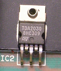
PDF TDA2030 Data sheet ( Hoja de datos )
| Número de pieza | TDA2030 | |
| Descripción | 14W Hi-Fi AUDIO AMPLIFIER | |
| Fabricantes | ST Microelectronics | |
| Logotipo | ||
 1. Hi-Fi Audio Amplifier - ST Hay una vista previa y un enlace de descarga de TDA2030 (archivo pdf) en la parte inferior de esta página. Total 17 Páginas | ||
|
No Preview Available !
TDA2030
14 W hi-fi audio amplifier
Features
■ Wide-range supply voltage, up to 36 V
■ Single or split power supply
■ Short-circuit protection to ground
■ Thermal shutdown
Description
The TDA2030 is a monolithic integrated circuit in
the Pentawatt® package, intended for use as a
low frequency class-AB amplifier. Typically it
provides 14 W output power (d = 0.5%) at
14 V/4 Ω. At ±14 V or 28 V, the guaranteed output
power is 12 W on a 4 Ω load and 8 W on an 8 Ω
(DIN45500).
The TDA2030 provides high output current and
has very low harmonic and crossover distortion.
Furthermore, the device incorporates an original
(and patented) short-circuit protection system
comprising an arrangement for automatically
limiting the dissipated power so as to keep the
operating point of the output transistors within
their safe operating range. A conventional thermal
shutdown system is also included.
Figure 1. Ex: Functional block diagram
Pentawatt (horizontal)
Table 1. Device summary
Order code
Package
TDA2030H
Pentawatt horizontal
June 2011
Doc ID 1458 Rev 3
1/17
www.st.com
17
1 page 
TDA2030
2.4 Characterizations
Electrical specifications
Figure 4. Output power vs. supply voltage Figure 5. Output power vs. supply voltage
Figure 6. Distortion vs. output power
Figure 7. Distortion vs. output power
Doc ID 1458 Rev 3
5/17
5 Page 
TDA2030
Practical considerations
Table 6. Single supply application
Component
R1
R2
R3
R4
RA/RB
C1
C2
C3
C5
C7
Recommanded
value
Purpose
Larger than
Smaller than
recommanded value recommanded value
150 kΩ
4.7 kΩ
Closed loop gain setting
Closed loop gain setting
Increase in gain
Decrease in gain(1)
Decrease in gain(1)
Increase in gain
100 kΩ
Non-inverting input biasing
Increase of input
impedance
Decrease in input
Impedance
1 Ω Frequency stability
Danger of oscillation at
high frequencies with
inductive loads
100 kΩ
Non-inverting input biasing
Poor high-frequency
attenuation
Danger of oscillation
1 µF
Input DC decoupling
Increase in low-
frequency cutoff
22 µF
Inverting DC decoupling
Increase in low-
frequency cutoff
0.1 µF
Supply voltage bypass
Danger of oscillation
100 µF
Supply voltage bypass
Danger of oscillation
0.22 µF
Frequency stability
Danger of oscillation
C8
--------1----------
2πBR1
Upper frequency cutoff
Smaller bandwidth
Larger bandwidth
D1D2
1N4001
To protect the device against output voltage spikes.
1. Closed loop gain must be higher than 24 dB
Doc ID 1458 Rev 3
11/17
11 Page | ||

| Páginas | Total 17 Páginas | |
| PDF Descargar | [ Datasheet TDA2030.PDF ] | |
Hoja de datos destacado
| Número de pieza | Descripción | Fabricantes |
| TDA2030 | 14W HI-FI AUDIO AMPLIFIER | Unisonic Technologies |
| TDA2030 | 14W Hi-Fi AUDIO AMPLIFIER | ST Microelectronics |
| TDA2030 | 18W Hi-Fi AMPLIFIER AND 35W DRIVER | WISWOOD |
| TDA2030A | 18W Hi-Fi AMPLIFIER AND 35W DRIVER | ST Microelectronics |
| Número de pieza | Descripción | Fabricantes |
| SLA6805M | High Voltage 3 phase Motor Driver IC. |
Sanken |
| SDC1742 | 12- and 14-Bit Hybrid Synchro / Resolver-to-Digital Converters. |
Analog Devices |
|
DataSheet.es es una pagina web que funciona como un repositorio de manuales o hoja de datos de muchos de los productos más populares, |
| DataSheet.es | 2020 | Privacy Policy | Contacto | Buscar |