|
|
|
PDF TC7650 Data sheet ( Hoja de datos )
| Número de pieza | TC7650 | |
| Descripción | CHOPPER-STABILIZED OPERATIONAL AMPLIFIER | |
| Fabricantes | TelCom Semiconductor | |
| Logotipo | ||
Hay una vista previa y un enlace de descarga de TC7650 (archivo pdf) en la parte inferior de esta página. Total 7 Páginas | ||
|
No Preview Available !
1
TC7650
CHOPPER-STABILIZED OPERATIONAL AMPLIFIER
FEATURES
s Low Input Offset Voltage ......................... 0.7µV Typ
s Low Input Offset Voltage Drift ......... 0.05µV/°C Max
s Low Input Bias Current ............................ 10pA Max
s High Impedance Differential CMOS Inputs .... 1012Ω
s High Open-Loop Voltage Gain ................ 120dB Min
s Low Input Noise Voltage ............................ 2.0µVp-p
s High Slew Rate .......................................... 2.5V/µsec
s Low-Power Operation ..................................... 20mW
s Output Clamp Speeds Recovery Time
s Compensated Internally for Stable Unity Gain
Operation
s Direct Replacement for ICL7650
s Available in 8-Pin Dip and 14-Pin Dip
ORDERING INFORMATION
Part No.
TC7650CPA
TC7650CPD
Package
8-Pin Plastic DIP
14-Pin Plastic DIP
Temperature
Range
0°C to +70°C
0°C to +70°C
Max
VOS
5µV
5µV
GENERAL DESCRIPTION
The TC7650 CMOS chopper-stabilized operational
amplifier practically removes offset voltage error terms
from system error calculations. The 5µV maximum VOS
specification, for example, represents a 15 times improve-
ment over the industry-standard OP07E. The 50nV/°C off-
set drift specification is over 25 times lower than the OP07E.
The increased performance eliminates VOS trim proce-
dures, periodic potentiometer adjustment and the reliability
problems caused by damaged trimmers.
The TC7650 performance advantages are achieved
without the additional manufacturing complexity and cost
incurred with laser or "zener zap" VOS trim techniques.
The TC7650 nulling scheme corrects both DC VOS
errors and VOS drift errors with temperature. A nulling
amplifier alternately corrects its own VOS errors and the main
amplifier VOS error. Offset nulling voltages are stored on two
user-supplied external capacitors. The capacitors connect
to the internal amplifier VOS null points. The main amplifier
input signal is never switched. Switching spikes are not
present at the TC7650 output.
The 14-pin dual-in-line package (DIP has an external
oscillator input to drive the nulling circuitry for optimum noise
performance. Both the 8 and 14-pin DIPs have an output
voltage clamp circuit to minimize overload recovery time.
2
3
4
5
FUNCTIONAL BLOCK DIAGRAM
OUTPUT
CLAMP
INPUTS
OUTPUT CLAMP
CIRCUIT
MAIN
AMPLIFIER
NULL
B
A
INTERMOD
COMPENSATION
B
NULL
AMPLIFIER
NULL
* FOR 8-PIN DIP, CONNECT TO VSS.
OSCILLATOR
14-PIN DIP ONLY
INT/EXT
EXT CLK IN
CLK OUT
AB
CEXT
OUTPUT
BA
CEXT
TC7650
*CRET
TELCOM SEMICONDUCTOR, INC.
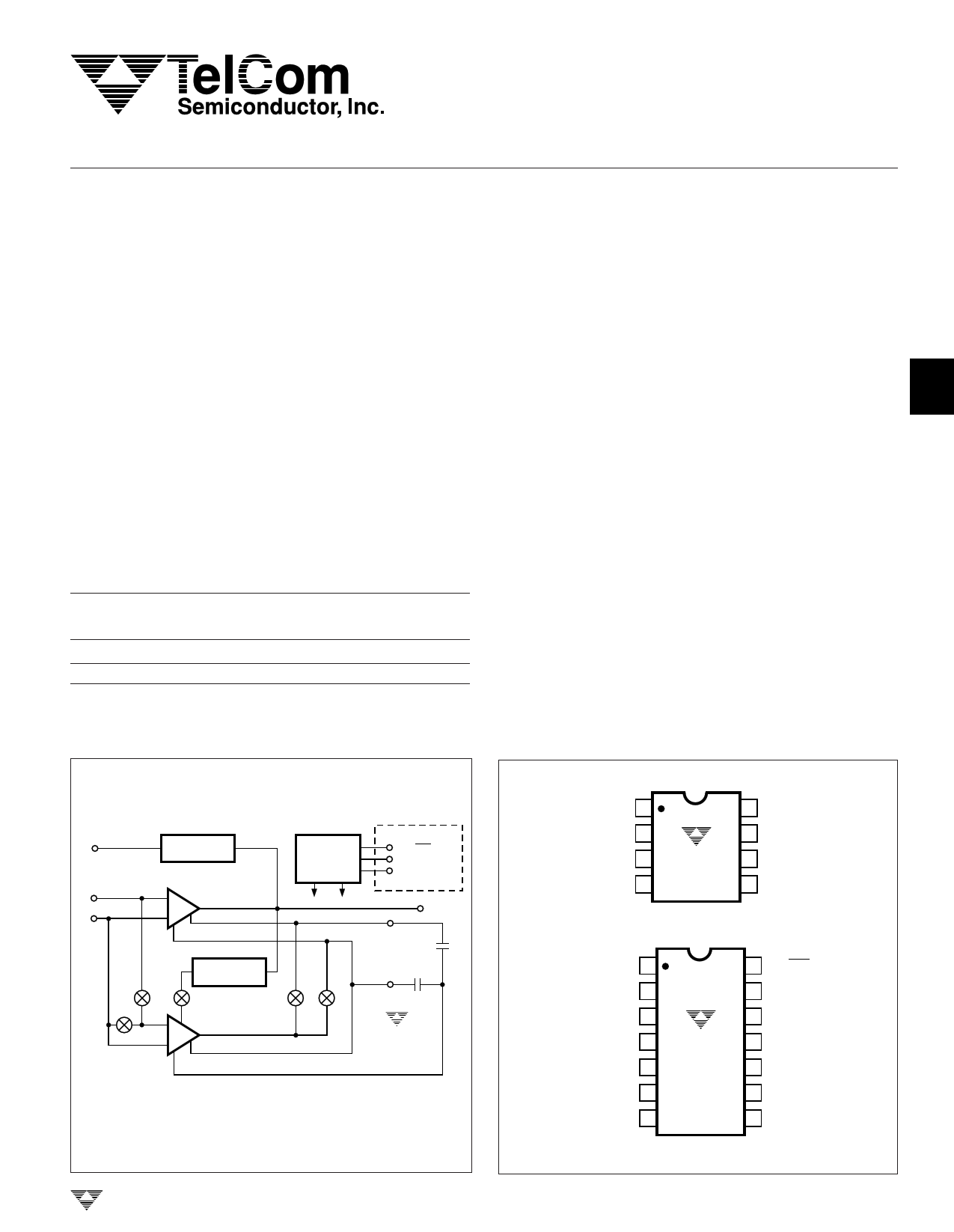
PIN CONFIGURATIONS
8-Pin DIP
CA 1
(–) INPUT 2
(+) INPUT 3
VSS 4
TC7650CPA
8 CB
7 VDD
6 OUTPUT
5 CLAMP
6
14-Pin DIP
CB 1
CA 2
NC
(GUARD)
3
(–) INPUT 4
(+) INPUT 5
NC
(GUARD)
6
VSS 7
TC7650CPD
14 INT/EXT
13
EXT CLK
INPUT
12
INT CLK
OUTPUT
11 VDD
10 OUTPUT
9
OUTPUT
CLAMP
8 CRETN
NC = NO INTERNAL CONNECTION
TC7650-5 9/11/96
3-273
7
8
1 page 
CHOPPER-STABILIZED
OPERATIONAL AMPLIFIER
1
TC7650
eliminates the overload recovery problem by reducing the
feedback network gain before the output voltage reaches
either supply rail.
INTERNAL
POSITIVE CLAMP BIAS
≈
V+ –VT ≈
V + – 0.7V
P-CHANNEL
OUTPUT
CLAMP PIN
N-CHANNEL
INTERNAL
NEGATIVE CLAMP BIAS ≈
≈
V
V
–
–
+
+
VT
0.7V
TC7650
OUTPUT PIN
Figure 3. Internal Clamp Circuit
*CONNECT TO VSS
ON 8-PIN DIP.
0.1µF
INPUT
C*
+R
C
–
CLAMP
R3 + ( R1/ R2 ) ≥ 100k Ω
FOR FULL CLAMP EFFECT.
R3
TC7650
OUTPUT
R2
R1
Figure 4. Noninverting Amplifier With Optional Clamp
R1
INPUT
*CONNECT TO VR–
ON 8-PIN DIP.
R2
CLAMP
TC7650
–
C
+ R*
OUTPUT
C ( R1 R2 ) ≥ 100kΩ
FOR FULL CLAMP
EFFECT.
0.1 µF 0.1 µF
Figure 5. Inverting Amplifier with Optional Clamp
TELCOM SEMICONDUCTOR, INC.
The output clamp circuit is shown in Figure 3, with typical
inverting and noninverting circuit connections shown in
Figures 4 and 5. Output voltage versus clamp circuit current
characteristics are shown in the typical operating curves.
For the clamp to be fully effective, the impedance across the
clamp output should be greater than 100kΩ.
2
Latch-Up Avoidance
Junction-isolated CMOS circuits inherently include a
parasitic 4-layer (p-n-p-n) structure which has characteris-
tics similar to an SCR. Under certain circumstances this
junction may be triggered into a low-impedance state, result-
ing in excessive supply current. To avoid this condition, no
voltage greater than 0.3V beyond the supply rails should be
applied to any pin. In general, the amplifier supplies must be
established either at the same time or before any input
signals are applied. If this is not possible, the drive circuits
must limit input current flow to under 0.1mA to avoid latch-
up.
3
4
Thermoelectric Potentials
Precision DC measurements are ultimately limited by
thermoelectric potentials developed in thermocouple junc-
tions of dissimilar metals, alloys, silicon, etc. Unless all
junctions are at the same temperature, thermoelectric volt-
ages, typically around 0.1µV/°C, but up to tens of µV/°C for
some materials, will be generated. In order to realize the
benefits extremely-low offset voltages provide, it is essential
to take special precautions to avoid temperature gradients.
All components should be enclosed to eliminate air move-
ment, especially those caused by power-dissipating ele-
ments in the system. Low thermoelectric-coefficient con-
nections should be used where possible and power supply
voltages and power dissipation should be kept to a mini-
mum. High-impedance loads are preferable, and separation
from surrounding heat-dissipating elements is advised.
5
6
Pin Compatibility
On the 8-pin mini-DIP TC7650, the external null storage
capacitors are connected to pins 1 and 8. On most other
operational amplifiers these are left open or are used for
offset potentiometer or compensation capacitor connec-
tions.
For OP05 and OP07 operational amplifiers, the replace-
ment of the offset null potentiometer between pins 1 and 8
by two capacitors from the pins to VSS will convert the OP05/
07 pin configurations for TC7650 operation. For LM108
devices, the compensation capacitor is replaced by the
external nulling capacitors. The LM101/748/709 pinouts
are modified similarly by removing any circuit connections to
pin 5. On the TC7650, pin 5 is the output clamp connection.
7
8
3-277
5 Page | ||
| Páginas | Total 7 Páginas | |
| PDF Descargar | [ Datasheet TC7650.PDF ] | |
Hoja de datos destacado
| Número de pieza | Descripción | Fabricantes |
| TC7650 | CHOPPER-STABILIZED OPERATIONAL AMPLIFIER | TelCom Semiconductor |
| TC7650 | Chopper Stabilized Operational Amplifier | Microchip Technology |
| TC7650CPA | Chopper Stabilized Operational Amplifier | Microchip Technology |
| TC7650CPA | CHOPPER-STABILIZED OPERATIONAL AMPLIFIER | TelCom Semiconductor |
| Número de pieza | Descripción | Fabricantes |
| SLA6805M | High Voltage 3 phase Motor Driver IC. |
Sanken |
| SDC1742 | 12- and 14-Bit Hybrid Synchro / Resolver-to-Digital Converters. |
Analog Devices |
|
DataSheet.es es una pagina web que funciona como un repositorio de manuales o hoja de datos de muchos de los productos más populares, |
| DataSheet.es | 2020 | Privacy Policy | Contacto | Buscar |