|
|
|
PDF 74LCX240MSA Data sheet ( Hoja de datos )
| Número de pieza | 74LCX240MSA | |
| Descripción | Low Voltage Octal Buffer/Line Driver with 5V Tolerant Inputs and Outputs | |
| Fabricantes | Fairchild Semiconductor | |
| Logotipo | ||
Hay una vista previa y un enlace de descarga de 74LCX240MSA (archivo pdf) en la parte inferior de esta página. Total 9 Páginas | ||
|
No Preview Available !
February 1994
Revised April 1999
74LCX240
Low Voltage Octal Buffer/Line Driver with
5V Tolerant Inputs and Outputs
General Description
The LCX240 is an inverting octal buffer and line driver
designed to be employed as a memory address driver,
clock driver and bus oriented transmitter or receiver. The
device is designed for low voltage (2.5V or 3.3V) VCC appli-
cations with capability of interfacing to a 5V signal environ-
ment.
The LCX240 is fabricated with an advanced CMOS tech-
nology to achieve high speed operation while maintaining
CMOS low power dissipation.
Features
s 5V tolerant inputs and outputs
s 2.3V–3.6V VCC specifications provided
s 6.5 ns tPD max (VCC = 3.3V), 10 µA ICC max
s Power-down high impedance inputs and outputs
s Supports live insertion/withdrawal (Note 1)
s ±24 mA output drive (VCC = 3.0V)
s Implements patented noise/EMI reduction circuitry
s Latch-up performance exceeds 500 mA
s ESD performance:
Human body model > 2000V
Machine model > 200V
Note 1: To ensure the high-impedance state during power up or down, OE
should be tied to VCC through a pull-up resistor: the minimum value or the
resistor is determined by the current-sourcing capability of the driver.
Ordering Code:
Order Number Package Number
Package Description
74LCX240WM
M20B
20-Lead Small Outline Integrated Circuit (SOIC), JEDEC MS-013, 0.300” Wide
74LCX240SJ
M20D
20-Lead Small Outline Package (SOP), EIAJ TYPE II, 5.3mm Wide
74LCX240MSA
MSA20
20-Lead Shrink Small Outline Package (SSOP), EIAJ TYPE II, 5.3mm Wide
74LCX240MTC
MTC20
20-Lead Thin Shrink Small Outline Package (TSSOP), JEDEC MO-153, 4.4mm Wide
Devices also available in Tape and Reel. Specify by appending the suffix letter “X” to the ordering code.
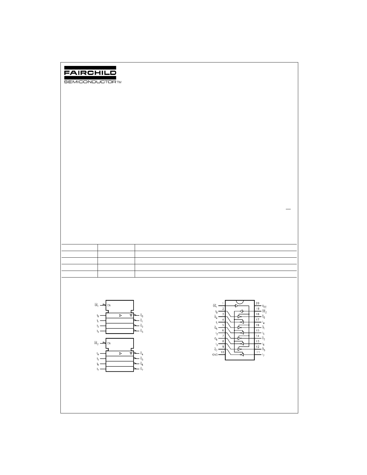
Logic Diagram
Connection Diagram
© 1999 Fairchild Semiconductor Corporation DS011993.prf
www.fairchildsemi.com
1 page 
AC Loading and Waveforms Generic for LCX Family
FIGURE 1. AC Test Circuit
(CL includes probe and jig capacitance)
Test
tPLH, tPHL
tPZL, tPLZ
tPZH,tPHZ
Switch
Open
6V at VCC = 3.3 ± 0.3V
VCC x 2 at VCC = 2.5 ± 0.2V
GND
Waveform for Inverting and Non-Inverting Functions
3-STATE Output Low Enable and
Disable Times for Logic
Propagation Delay, Pulse Width and trec Waveforms
Setup Time, Hold TIme and Recovery TIme for Logic
3-STATE Output High Enable and
Disable TImes for Logic
trise and tfall
FIGURE 2. Waveforms
(Input Pulse Characteristics; f=1MHz, tr=tf=3ns)
Symbol
Vmi
Vmo
Vx
Vy
VCC
3.3V ± 0.3V
1.5V
1.5V
VOL + 0.3V
VOH − 0.3V
2.7V
1.5V
1.5V
VOL + 0.3V
VOH − 0.3V
2.5V ± 0.2V
VCC/2
VCC/2
VOL + 0.15V
VOH − 0.15V
5 www.fairchildsemi.com
5 Page | ||
| Páginas | Total 9 Páginas | |
| PDF Descargar | [ Datasheet 74LCX240MSA.PDF ] | |
Hoja de datos destacado
| Número de pieza | Descripción | Fabricantes |
| 74LCX240MSA | Low Voltage Octal Buffer/Line Driver with 5V Tolerant Inputs and Outputs | Fairchild Semiconductor |
| Número de pieza | Descripción | Fabricantes |
| SLA6805M | High Voltage 3 phase Motor Driver IC. |
Sanken |
| SDC1742 | 12- and 14-Bit Hybrid Synchro / Resolver-to-Digital Converters. |
Analog Devices |
|
DataSheet.es es una pagina web que funciona como un repositorio de manuales o hoja de datos de muchos de los productos más populares, |
| DataSheet.es | 2020 | Privacy Policy | Contacto | Buscar |