|
|
|
PDF IDT74FCT32932-100PA Data sheet ( Hoja de datos )
| Número de pieza | IDT74FCT32932-100PA | |
| Descripción | 3.3V LOW SKEW PLL-BASED CMOS CLOCK DRIVER | |
| Fabricantes | Integrated Device Tech | |
| Logotipo | ||
Hay una vista previa y un enlace de descarga de IDT74FCT32932-100PA (archivo pdf) en la parte inferior de esta página. Total 9 Páginas | ||
|
No Preview Available !
IDT74FCT3932-100, IDT74FCT32932-100
LOW SKEW PLL-BASED CLOCK DRIVER
Integrated Device Technology, Inc.
COMMERCIDIATL 7TE4MFPCERTA3T9UR3E2R-1A0NG0ES
3.3V LOW SKEW PLL-BASED
IDT74FCT32932-100
CMOS CLOCK DRIVER
ADVANCE INFORMATION
FEATURES:
• 0.5 MICRON CMOS Technology
• Guaranteed low skew
• 16 programmable frequency configurations
• 17 3-state outputs: ±24 mA FCT3932
±8 mA FCT32932
• Output configuration:
BANK1: 4 outputs
BANK2: 8 outputs
BANK3: 5 outputs
• Dedicated feedback output (Q_FB)
• Maximum output frequency: 100MHz
• VCC = 3.3V ±0.3V
• Inputs can be driven from 3.3V or 5V components
• Available in 48 SSOP, TSSOP packages
• Suited to SDRAM applications
DESCRIPTION:
The FCT3932 uses phase-lock loop technology to lock the
frequency and phase of the feedback to the input reference
clock. It provides a large number of low skew outputs that are
configurable in 16 different modes using the CNTRL 1-4
inputs. A dedicated output, Q_FB, is provided to supply the
PLL feedback and it should be connected to the FEEDBACK
input. Q_FB is located adjacent to FEEDBACK to minimize
the delay in the feedback path. In order to offset any delay in
the output path from the FCT3932 output to a receiving device,
feedback path delay should be made to match this output path
delay.
The PLL consists of the phase/frequency detector, charge
pump, loop filter and VCO. The FCT3932 requires no external
loop filter components.
The FCT3932 provides 17 outputs grouped in 3 banks with
individual 3-state control and an additional dedicated feed-
back output with no disable. Connecting Q_FB to FEEDBACK
ensures uninterrupted PLL operation when all outputs are
disabled.
Individual bank 3-state allows users to disable unused
outputs in order to limit power dissipation or minimize switch-
ing noise. It also allows users to shut down outputs in low
power modes while maintaining phase lock.
The FCT3932 provides a LOCK pin that goes high when the
device is phase-locked.
The user can bypass the PLL for testability purposes by
deasserting PLL_EN. In this "test" mode, the input frequency
is not limited to the specified range.
RSTThe FCT3932 provides an asynchronous reset input, ,
which resets all outputs. This initializes all internal registers so
that outputs start up in a known state.
APPLICATIONS:
SDRAM DIMM Clock, Caches, high speed microproces-
sors, motherboard clock distribution to DIMMs.
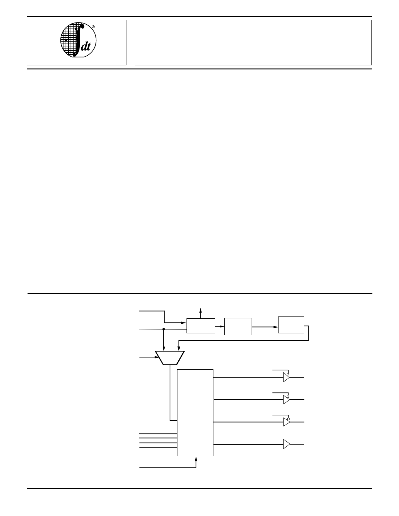
FUNCTIONAL BLOCK DIAGRAM
FEEDBACK
REF_IN
LOCK
Phase/Freq.
Detector
Charge
Pump &
Loop Filter
Voltage
Controlled
Oscillator
PLL_EN
01
Mux
CNTRL1-4
C
O
N
T
R
O
L
OE1
OE2
OE3
Q41-4
(BANK 1)
Q81-8
(BANK 2)
Q51-5
(BANK 3)
Q_FB
RST
The IDT logo is a registered trademark of Integrated Device Technology, Inc.
COMMERCIAL TEMPERATURE RANGE
©1996 Integrated Device Technology, Inc.
9.9
9.9
3267 drw 01
NOVEMBER 1996
DSC-3267/2
11
1 page 
IDT74FCT3932-100, IDT74FCT32932-100
LOW SKEW PLL-BASED CLOCK DRIVER
COMMERCIAL TEMPERATURE RANGES
INPUT TIMING REQUIREMENTS
Symbol
tRISE/FALL
Frequency
Duty Cycle
Parameter
Rise/Fall Times REF_IN input (0.8V to 2.0V)
Input Frequency REF_IN input Modes 0, 1, 2, 3, 4
Modes 5, 6, 7
Modes 8, 9, 10, 11, 12
Modes 13, 14, 15
Input Duty Cycle, REF_IN input
OUTPUT FREQUENCY SPECIFICATIONS
Mode
0, 1, 2, 3,4
Parameter
Operating
F, F Outputs
frequency
F/2 Outputs
F/3 Outputs
5, 6, 7
Operating
3F Outputs
frequency
F Outputs
8, 9, 10, 11, 12
Operating
2F Outputs
frequency
F Outputs
F/2 Outputs
13, 14, 15
Operating
4F Outputs
frequency
2F Outputs
F Outputs
Min.
—
50
16.7
25
12.5
25
Min.
50
25
16.7
50
16.7
50
25
12.5
50
25
12.5
Max.
3.0
100
33.3
50
25
75
Max.
100
50
33.3
100
33.3
100
50
25
100
50
25
Unit
ns
MHz
%
3267 tbl 09
Unit
MHz
3267 tbl 10
POWER SUPPLY CHARACTERISTICS
Symbol
∆ICC
ICCD
IC
Parameter
Quiescent Power Supply Current
TTL Inputs HIGH
Dynamic Power Supply
Current(4)
Total Power Supply Current(5,6)
VCC = Max.
Test Conditions(1)
VIN = VCC –0.6V(3)
Min. Typ.(2) Max.
— 2.0 30
VCC = Max.
VIN = VCC
All Outputs Open
VIN = GND
50% Duty Cycle
MODE 10
VCC = Max.
PLL_EN = 1, LOCK = 1, MODE 10
REF_IN frequency = 50MHz.
All outputs open
F = 50Mhz
—
—
72
62
Unit
µA
µA/
MHz/
bit
mA
NOTES:
3267 tbl 08
1. For conditions shown as Max. or Min., use appropriate value specified under Electrical Characteristics.
2. Typical values are at VCC = 3.3V, +25°C ambient.
3. Per TTL driven input; all other inputs at VCC or GND.
4. This parameter is not directly testable, but is derived for use in Total Power Supply Calculations. It is derived with Q frequency as the reference.
5. Values for these conditions are examples of the ICC formula. These limits are guaranteed but not tested.
6. IC = IQUIESCENT + IINPUTS + IDYNAMIC
IC = ICC + ∆ICC DHNT + ICCD (f) + ILOAD
ICC = Quiescent Current (ICCL, ICCH and ICCZ)
∆ICC = Power Supply Current for a TTL High Input
DH = Duty Cycle for TTL Inputs High
NT = Number of TTL Inputs at DH
ICCD = Dynamic Current Caused by an Input Transition Pair (HLH or LHL)
f = SYNC input frequency
ILOAD = Dynamic Current due to load.
9.9 5
5 Page | ||
| Páginas | Total 9 Páginas | |
| PDF Descargar | [ Datasheet IDT74FCT32932-100PA.PDF ] | |
Hoja de datos destacado
| Número de pieza | Descripción | Fabricantes |
| IDT74FCT32932-100PA | 3.3V LOW SKEW PLL-BASED CMOS CLOCK DRIVER | Integrated Device Tech |
| IDT74FCT32932-100PV | 3.3V LOW SKEW PLL-BASED CMOS CLOCK DRIVER | Integrated Device Tech |
| Número de pieza | Descripción | Fabricantes |
| SLA6805M | High Voltage 3 phase Motor Driver IC. |
Sanken |
| SDC1742 | 12- and 14-Bit Hybrid Synchro / Resolver-to-Digital Converters. |
Analog Devices |
|
DataSheet.es es una pagina web que funciona como un repositorio de manuales o hoja de datos de muchos de los productos más populares, |
| DataSheet.es | 2020 | Privacy Policy | Contacto | Buscar |