|
|
|
PDF IDT74FCT162260AT Data sheet ( Hoja de datos )
| Número de pieza | IDT74FCT162260AT | |
| Descripción | FAST CMOS 12-BIT TRI-PORT BUS EXCHANGER | |
| Fabricantes | Integrated Device Tech | |
| Logotipo | ||
Hay una vista previa y un enlace de descarga de IDT74FCT162260AT (archivo pdf) en la parte inferior de esta página. Total 8 Páginas | ||
|
No Preview Available !
Integrated Device Technology, Inc.
FAST CMOS
12-BIT TRI-PORT
BUS EXCHANGER
IDT54/74FCT16260AT/CT/ET
IDT54/74FCT162260AT/CT/ET
FEATURES:
• Common features:
– 0.5 MICRON CMOS Technology
– High-speed, low-power CMOS replacement for
ABT functions
– Typical tSK(o) (Output Skew) < 250ps
– Low input and output leakage ≤1µA (max.)
– ESD > 2000V per MIL-STD-883, Method 3015;
> 200V using machine model (C = 200pF, R = 0)
– Packages include 25 mil pitch SSOP, 19.6 mil pitch
TSSOP, 15.7 mil pitch TVSOP and 25 mil pitch Cerpack
– Extended commercial range of -40°C to +85°C
– VCC = 5V ±10%
• Features for FCT16260AT/CT/ET:
– High drive outputs (-32mA IOH, 64mA IOL)
– Power off disable outputs permit “live insertion”
– Typical VOLP (Output Ground Bounce) < 1.0V at
VCC = 5V, TA = 25°C
• Features for FCT162260AT/CT/ET:
– Balanced Output Drivers: ±24mA (commercial),
±16mA (military)
– Reduced system switching noise
– Typical VOLP (Output Ground Bounce) < 0.6V at
VCC = 5V,TA = 25°C
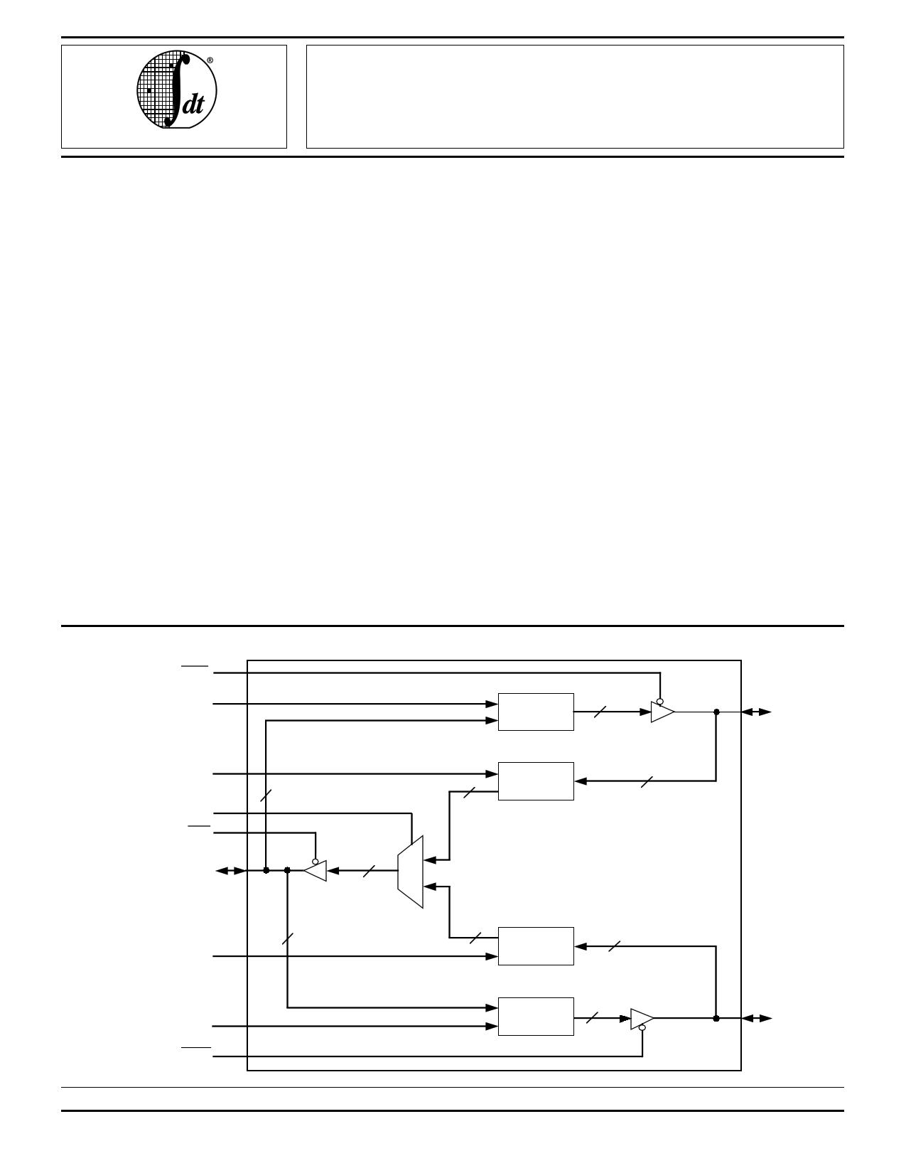
DESCRIPTION:
The FCT16260AT/CT/ET and the FCT162260AT/CT/ET
Tri-Port Bus Exchangers are high-speed 12-bit latched bus
multiplexers/transceivers for use in high-speed microproces-
sor applications. These Bus Exchangers support memory
interleaving with latched outputs on the B ports and address
multiplexing with latched inputs on the B ports.
The Tri-Port Bus Exchanger has three 12-bit ports. Data
may be transferred between the A port and either/both of the
B ports. The latch enable (LE1B, LE2B, LEA1B and LEA2B)
inputs control data storage. When a latch-enable input is
HIGH, the latch is transparent. When a latch-enable input is
LOW, the data at the input is latched and remains latched until
the latch enable input is returned HIGH. Independent output
enables (OE1B and OE2B) allow reading from one port while
writing to the other port.
The FCT16260AT/CT/ET are ideally suited for driving high
capacitance loads and low impedance backplanes. The
output buffers are designed with power off disable capability
to allow "live insertion" of boards when used as backplane
drivers.
The FCT162260AT/CT/ET have balanced output drive
with current limiting resistors. This offers low ground bounce,
minimal undershoot, and controlled output fall times - reduc-
ing the need for external series terminating resistors.
FUNCTIONAL BLOCK DIAGRAM
OE1B
LEA1B
A-1B
LATCH
12
1B1:12
LE1B
SEL
OEA
A1:12
12
LE2B
12
1B-A
LATCH
12
M1
U
12 X 0
12
2B-A
LATCH
12
12
LEA2B
OE2B
The IDT logo is a registered trademark of Integrated Device Technology, Inc.
MILITARY AND COMMERCIAL TEMPERATURE RANGES
©1996 Integrated Device Technology, Inc.
5.4
A-2B
LATCH
12
2B1:12
3032 drw 01
AUGUST 1996
DSC-3032/6
1
1 page 
IDT54/74FCT16260AT/CT/ET, 162260AT/CT/ET
FAST CMOS 12-BIT TRI-PORT BUS EXCHANGER
MILITARY AND COMMERCIAL TEMPERATURES RANGES
POWER SUPPLY CHARACTERISTICS
Symbol
Parameter
Test Conditions(1)
Min. Typ.(2) Max. Unit
∆ICC
Quiescent Power Supply Current VCC = Max.
TTL Inputs HIGH
VIN = 3.4V(3)
— 0.5 1.5 mA
ICCD
Dynamic Power Supply Current(4) VCC = Max.
VIN = VCC
— 60 100 µA/
Outputs Open
VIN = GND
MHz
One Output Port Enabled
LExx = VCC
One Input Bit Toggling
One Output Bit Toggling
50% Duty Cycle
IC
Total Power Supply Current(6)
VCC = Max.
VIN = VCC
— 0.6 1.5 mA
Outputs Open
VIN = GND
fi = 10MHz
50% Duty Cycle
VIN = 3.4V
— 0.9 2.3
One Output Port Enabled
VIN = GND
LExx = VCC
One Input Bit Toggling
One Output Bit Toggling
VCC = Max.
VIN = VCC
— 1.8 3.5(5)
Outputs Open
VIN = GND
fi = 2.5MHz
50% Duty Cycle
VIN = 3.4V
— 4.8 12.5(5)
One Output Port Enabled
VIN = GND
LExx = VCC
Twelve Input Bits Toggling
Twelve Output Bits Toggling
NOTES:
3032 tbl 09
1. For conditions shown as Max. or Min., use appropriate value specified under Electrical Characteristics for the applicable device type.
2. Typical values are at VCC = 5.0V, +25°C ambient.
3. Per TTL driven input (VIN = 3.4V). All other inputs at VCC or GND.
4. This parameter is not directly testable, but is derived for use in Total Power Supply Calculations.
5. Values for these conditions are examples of the ICC formula. These limits are guaranteed but not tested.
6. IC = IQUIESCENT + IINPUTS + IDYNAMIC
IC = ICC + ∆ICC DHNT + ICCD (fCPNCP/2 + fiNi)
ICC = Quiescent Current (ICCL, ICCH and ICCZ)
∆ICC = Power Supply Current for a TTL High Input (VIN = 3.4V)
DH = Duty Cycle for TTL Inputs High
NT = Number of TTL Inputs at DH
ICCD = Dynamic Current Caused by an Input Transition Pair (HLH or LHL)
fCP = Clock Frequency for Register Devices (Zero for Non-Register Devices)
NCP = Number of Clock Inputs at fCP
fi = Input Frequency
Ni = Number of Inputs at fi
5.4 5
5 Page | ||
| Páginas | Total 8 Páginas | |
| PDF Descargar | [ Datasheet IDT74FCT162260AT.PDF ] | |
Hoja de datos destacado
| Número de pieza | Descripción | Fabricantes |
| IDT74FCT162260AT | FAST CMOS 12-BIT TRI-PORT BUS EXCHANGER | Integrated Device Tech |
| Número de pieza | Descripción | Fabricantes |
| SLA6805M | High Voltage 3 phase Motor Driver IC. |
Sanken |
| SDC1742 | 12- and 14-Bit Hybrid Synchro / Resolver-to-Digital Converters. |
Analog Devices |
|
DataSheet.es es una pagina web que funciona como un repositorio de manuales o hoja de datos de muchos de los productos más populares, |
| DataSheet.es | 2020 | Privacy Policy | Contacto | Buscar |