|
|
|
PDF IDT72V3622 Data sheet ( Hoja de datos )
| Número de pieza | IDT72V3622 | |
| Descripción | 3.3 VOLT CMOS SyncBiFIFO 256 x 36 x 2 512 x 36 x 2 1/024 x 36 x 2 | |
| Fabricantes | Integrated Device Tech | |
| Logotipo | ||
Hay una vista previa y un enlace de descarga de IDT72V3622 (archivo pdf) en la parte inferior de esta página. Total 29 Páginas | ||
|
No Preview Available !
3.3 VOLT CMOS SyncBiFIFOTM
256 x 36 x 2
512 x 36 x 2
1,024 x 36 x 2
IDT72V3622
IDT72V3632
IDT72V3642
.EATURES:
• Memory storage capacity:
IDT72V3622 – 256 x 36 x 2
IDT72V3632 – 512 x 36 x 2
IDT72V3642 – 1,024 x 36 x 2
• Supports clock frequencies up to 100 MHz
• Fast access times of 6.5ns
• Free-running CLKA and CLKB may be asynchronous or coincident
(simultaneous reading and writing of data on a single clock edge
is permitted)
• Two independent clocked FIFOs buffering data in opposite direc-
tions
• Mailbox bypass register for each FIFO
• Programmable Almost-Full and Almost-Empty flags
• Microprocessor Interface Control Logic
• FFA/IRA, EFA/ORA, AEA, and AFA flags synchronized by CLKA
• FFB/IRB, EFB/ORB, AEB, and AFB flags synchronized by CLKB
• Select IDT Standard timing (using EFA, EFB, FFA and FFB flags
functions) or First Word Fall Through timing (using ORA, ORB, IRA
and IRB flag functions)
• Available in 132-pin Plastic Quad Flatpack (PQFP) or space-saving
120-pin Thin Quad Flatpack (TQFP)
• Functionally compatible to the 5V operating IDT723622/723632/
723642
• Industrial temperature range (–40οC to +85οC) is available
DESCRIPTION:
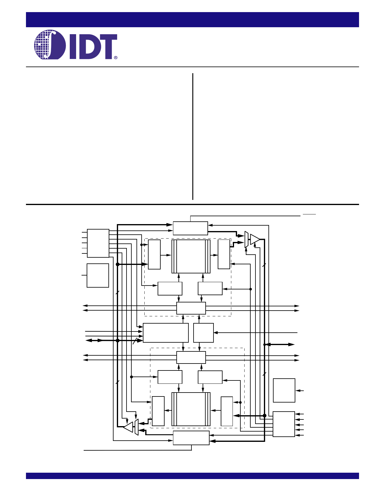
The IDT72V3622/72V3632/72V3642 are functionally compatible versions
of the IDT723622/723632/723642, designed to run off a 3.3V supply for
exceptionally low-power consumption. These devices are monolithic, high-
speed, low-power, CMOS Bidirectional SyncFIFO (clocked) memories which
support clock frequencies up to 100MHz and have read access times as fast
as 6.5ns. Two independent 256/512/1,024 x 36 dual-port SRAM FIFOs on
board each chip buffer data in opposite directions. Communication between
.UNCTIONAL BLOCK DIAGRAM
CLKA
CSA
W/RA
ENA
MBA
Port-A
Control
Logic
RST1
FIFO1,
Mail1
Reset
Logic
36
Mail 1
Register
RAM
ARRAY
256 x 36
512 x 36
1,024 x 36
Write
Pointer
Read
Pointer
MBF1
36
FFA/IRA
AFA
FIFO 1
Status Flag
Logic
EFB/ORB
AEB
FS0
FS1
A0 - A35
EFA/ORA
AEA
Programmable Flag Timing
Offset Registers
Mode
10
FIFO 2
Status Flag
Logic
Read
Write
36
Pointer
Pointer
RAM
ARRAY
256 x 36
512 x 36
1,024 x 36
MBF2
Mail 2
Register
IDT, the IDT logo are registered trademarks of Integrated Device Technology, Inc. SyncBiFIFO is a trademark of Integrated Device Technology, Inc.
COMMERCIAL TEMPERATURE RANGE
1
2001 Integrated Device Technology, Inc. All rights reserved. Product specifications subject to change without notice.
FWFT
B0 - B35
FFB/IRB
AFB
36
FIFO2,
Mail2
Reset
Logic
RST2
Port-B
Control
Logic
CLKB
CSB
W/RB
ENB
MBB
4660 drw 01
DECEMBER 2001
DSC-4660/4
1 page 
IDT72V3622/72V3632/72V3642 CMOS 3.3V SyncBiFIFOTM
256 x 36 x 2, 512 x 36 x 2, 1,024 x 36 x 2
PIN DESCRIPTIONS (CONTINUED)
COMMERCIAL TEMPERATURERANGE
Symbol
Name
I/O
Description
MBA Port A Mailbox I A HIGH level on MBA chooses a mailbox register for a port A read or write operation. When the
Select
A0-A35 outputs are active, a HIGH level on MBA selects data from the mail2 register for output and a
LOW level selects FIFO2 output register data for output.
MBB
MBF1
Port B Mailbox
Select
Mail1 Register
Flag
MBF2
Mail2 Register
Flag
RST1
FIFO1 Reset
RST2
FIFO2 Reset
W/RA
W/RB
Port A Write/
Read Select
Port B Write/
Read Select
I A HIGH level on MBB chooses a mailbox register for a port B read or write operation. When the
B0-B35 outputs are active, a HIGH level on MBB selects data from the mail1 register or output and a
LOW level selects FIFO1 output register data for output.
O MBF1 is set LOW by a LOW-to-HIGH transition of CLKA that writes data to the mail1 register.
Writes to the mail1 register are inhibited while MBF1 is LOW. MBF1 is set HIGH by a LOW-to-HIGH
transition of CLKB when a port B read is selected and MBB is HIGH. MBF1 is set HIGH when FIFO1
is reset.
O MBF2 is set LOW by a LOW-to-HIGH transition of CLKB that writes data to the mail2 register. Writes
to the mail2 register are inhibited while MBF2 is LOW. MBF2 is set HIGH by a LOW-to-HIGH
transition of CLKA when a port A read is selected and MBA is HIGH. MBF2 is also set HIGH when
FIFO2 is reset.
I ToresetFIFO1,fourLOW-to-HIGHtransitionsofCLKAandfourLOW-to-HIGHtransitionsofCLKBmustoccur
while RST1 is LOW. The LOW-to-HIGH transition of RST1 latches the status of FS0 and FS1 for AFA
and AEB offset selection. FIFO1 must be reset upon power up before data is written to its RAM.
I ToresetFIFO2,fourLOW-to-HIGHtransitionsofCLKAandfourLOW-to-HIGHtransitionsofCLKBmustoccur
while RST2 is LOW. The LOW-to-HIGH transition of RST2 latches the status of FS0 and FS1 for AFB
and AEA offset selection. FIFO2 must be reset upon power up before data is written to its RAM.
I A HIGH selects a write operation and a LOW selects a read operation on port A for a LOW-to-HIGH
transition of CLKA. The A0-A35 outputs are in the HIGH impedance state when W/RA is HIGH.
I A LOW selects a write operation and a HIGH selects a read operation on port B for a LOW-to-HIGH
transition of CLKB. The B0-B35 outputs are in the HIGH impedance state when W/RB is LOW.
5
5 Page 
IDT72V3622/72V3632/72V3642 CMOS 3.3V SyncBiFIFOTM
256 x 36 x 2, 512 x 36 x 2, 1,024 x 36 x 2
FIFO WRITE/READ OPERATION
The state of the port A data (A0-A35) outputs is controlled by port A Chip
Select (CSA) and port A Write/Read select (W/RA). The A0-A35 outputs are
in the high-impedance state when either CSA or W/RA is HIGH. The A0-A35
outputs are active when both CSA and W/RA are LOW.
Data is loaded into FIFO1 from the A0-A35 inputs on a LOW-to-HIGH
transition of CLKA when CSA is LOW, W/RA is HIGH, ENA is HIGH , MBA is
LOW, and FFA/IRA is HIGH. Data is read from FIFO2 to the A0-A35 outputs
byaLOW-to-HIGHtransitionofCLKAwhen CSAis LOW, W/RAisLOW,ENA
is HIGH, MBA is LOW, and EFA/ORA is HIGH (see Table 2). FIFO reads and
writes on port A are independent of any concurrent port B operation. Write and
Read cycle timing diagrams for Port A can be found in Figure 4 and 7.
The port B control signals are identical to those of port A with the exception
that the port B Write/Read select (W/RB) is the inverse of the port A Write/Read
select (W/RA). The state of the port B data (B0-B35) outputs is controlled by the
port B Chip Select (CSB) and port B Write/Read select (W/RB). The B0-B35
outputs are in the high-impedance state when either CSB is HIGH or W/RB
isLOW.TheB0-B35outputsareactivewhen CSBisLOWandW/RBisHIGH.
Data is loaded into FIFO2 from the B0-B35 inputs on a LOW-to-HIGH
transition of CLKB when CSB is LOW, W/RB is LOW, ENB is HIGH, MBB is
LOW, and FFB/IRB is HIGH. Data is read from FIFO1 to the B0-B35 outputs
by a LOW-to-HIGH transition of CLKB when CSB is LOW, W/RB is HIGH, ENB
is HIGH, MBB is LOW, and EFB/ORB is HIGH (see Table 3) . FIFO reads and
writes on port B are independent of any concurrent port A operation. Write and
Read cycle timing diagrams for Port B can be found in Figure 5 and 6.
The setup and hold time constraints to the port Clocks for the port Chip
Selects and Write/Read selects are only for enabling write and read operations
COMMERCIAL TEMPERATURERANGE
and are not related to high-impedance control of the data outputs. If a port enable
is LOW during a clock cycle, the port’s Chip Select and Write/Read select may
change states during the setup and hold time window of the cycle.
When operating the FIFO in FWFT mode and the Output Ready flag is LOW,
the next word written is automatically sent to the FIFO’s output register by the
LOW-to-HIGH transition of the port clock that sets the Output Ready flag HIGH.
When the Output Ready flag is HIGH, subsequent data is clocked to the output
registers only when a read is selected using the port’s Chip Select, Write/Read
select, Enable, and Mailbox select.
When operating the FIFO in IDT Standard mode, the first word will cause
the Empty Flag to change state on the second LOW-to-HIGH transition of the
ReadClock. Thedatawordwillnotbeautomaticallysenttotheoutputregister.
Instead, data residing in the FIFO's memory array is clocked to the output
register only when a read is selected using the port’s Chip Select, Write/Read
select, Enable, and Mailbox select.
SYNCHRONIZED FIFO FLAGS
Each FIFO is synchronized to its port clock through at least two flip-flop
stages. This is done to improve flag signal reliability by reducing the probability
of metastable events when CLKA and CLKB operate asynchronously to one
another. EFA/ORA, AEA, FFA/IRA, and AFA are synchronized to CLKA.
EFB/ORB, AEB, FFB/IRB, and AFB are synchronized to CLKB. Tables
4 and 5 show the relationship of each port flag to FIFO1 and FIFO2.
EMPTY/OUTPUT READY FLAGS (EFA/ORA, EFB/ORB)
These are dual purpose flags. In the FWFT mode, the Output Ready
(ORA, ORB) function is selected. When the Output Ready flag is HIGH,
TABLE 2 PORT A ENABLE .UNCTION TABLE
CSA W/RA ENA
MBA CLKA
Data A (A0-A35) I/O
HXX X X
High-Impedance
LHL X X
Input
LHH L ↑
Input
LHH H ↑
Input
LLL L X
Output
LLH L ↑
Output
LLL H X
Output
LLH H ↑
Output
Port Function
None
None
FIFO1 write
Mail1 write
None
FIFO2 read
None
Mail2 read (set MBF2 HIGH)
TABLE 3 PORT B ENABLE .UNCTION TABLE
CSB W/RB
ENB
MBB CLKB
Data B (B0-B35) I/O
HXX X X
High-Impedance
LLL X X
Input
LLH L ↑
Input
LLH H ↑
Input
LHL L X
Output
LHH L ↑
Output
LHL H X
Output
LHH H ↑
Output
11
Port Function
None
None
FIFO2 write
Mail2 write
None
FIFO1 read
None
Mail1 read (set MBF1 HIGH)
11 Page | ||
| Páginas | Total 29 Páginas | |
| PDF Descargar | [ Datasheet IDT72V3622.PDF ] | |
Hoja de datos destacado
| Número de pieza | Descripción | Fabricantes |
| IDT72V3622 | 3.3 VOLT CMOS SyncBiFIFO 256 x 36 x 2 512 x 36 x 2 1/024 x 36 x 2 | Integrated Device Tech |
| IDT72V3623 | (IDT72V36x3) 3.3 VOLT CMOS SyncFIFO | Integrated Device Technology |
| IDT72V3624 | (IDT72V36x4) 3.3 VOLT CMOS SyncBiFIFO | Integrated Device Technology |
| IDT72V3626 | (IDT72V36x6) 3.3 VOLT CMOS TRIPLE BUS SyncFIFO | Integrated Device Technology |
| Número de pieza | Descripción | Fabricantes |
| SLA6805M | High Voltage 3 phase Motor Driver IC. |
Sanken |
| SDC1742 | 12- and 14-Bit Hybrid Synchro / Resolver-to-Digital Converters. |
Analog Devices |
|
DataSheet.es es una pagina web que funciona como un repositorio de manuales o hoja de datos de muchos de los productos más populares, |
| DataSheet.es | 2020 | Privacy Policy | Contacto | Buscar |