|
|
|
PDF IDT72V223 Data sheet ( Hoja de datos )
| Número de pieza | IDT72V223 | |
| Descripción | 3.3 VOLT HIGH-DENSITY SUPERSYNC NARROW BUS FIFO | |
| Fabricantes | Integrated Device Tech | |
| Logotipo | ||
Hay una vista previa y un enlace de descarga de IDT72V223 (archivo pdf) en la parte inferior de esta página. Total 30 Páginas | ||
|
No Preview Available !
3.3 VOLT HIGH-DENSITY SUPERSYNC II™
NARROW BUS FIFO
512 x 18/1,024 x 9, 1,024 x 18/2,048 x 9
2,048 x 18/4,096 x 9, 4,096 x 18/8,192 x 9
8,192 x 18/16,384 x 9, 16,384 x 18/32,768 x 9
32,768 x 18/65,536 x 9, 65,536 x 18/131,072 x 9
IDT72V223, IDT72V233
IDT72V243, IDT72V253
IDT72V263, IDT72V273
IDT72V283, IDT72V293
FEATURES:
• Choose among the following memory organizations:
IDT72V223 512 x 18/1,024 x 9
IDT72V233 1,024 x 18/2,048 x 9
IDT72V243 2,048 x 18/4,096 x 9
IDT72V253 4,096 x 18/8,192 x 9
IDT72V263 8,192 x 18/16,384 x 9
IDT72V273 16,384 x 18/32,768 x 9
IDT72V283 32,768 x 18/65,536 x 9
IDT72V293 65,536 x 18/131,072 x 9
• Functionally compatible with the IDT72V255LA/72V265LA and
IDT72V275/72V285 SuperSync FIFOs
• Up to 166 MHz Operation of the Clocks
• User selectable Asynchronous read and/or write ports (BGA Only)
• User selectable input and output port bus-sizing
- x9 in to x9 out
- x9 in to x18 out
- x18 in to x9 out
- x18 in to x18 out
• Pin to Pin compatible to the higher density of IDT72V2103/72V2113
• Big-Endian/Little-Endian user selectable byte representation
• 5V tolerant inputs
• Fixed, low first word latency
• Zero latency retransmit
• Auto power down minimizes standby power consumption
• Master Reset clears entire FIFO
• Partial Reset clears data, but retains programmable settings
• Empty, Full and Half-Full flags signal FIFO status
• Programmable Almost-Empty and Almost-Full flags, each flag can
default to one of eight preselected offsets
• Selectable synchronous/asynchronous timing modes for Almost-
Empty and Almost-Full flags
• Program programmable flags by either serial or parallel means
• Select IDT Standard timing (using EF and FF flags) or First Word
Fall Through timing (using OR and IR flags)
• Output enable puts data outputs into high impedance state
• Easily expandable in depth and width
• JTAG port, provided for Boundary Scan function (BGA Only)
• Independent Read and Write Clocks (permit reading and writing
simultaneously)
• Available in a 80-pin Thin Quad Flat Pack (TQFP) or a 100-pin Ball
Grid Array (BGA) (with additional features)
• High-performance submicron CMOS technology
• Industrial temperature range (–40°C to +85°C) is available
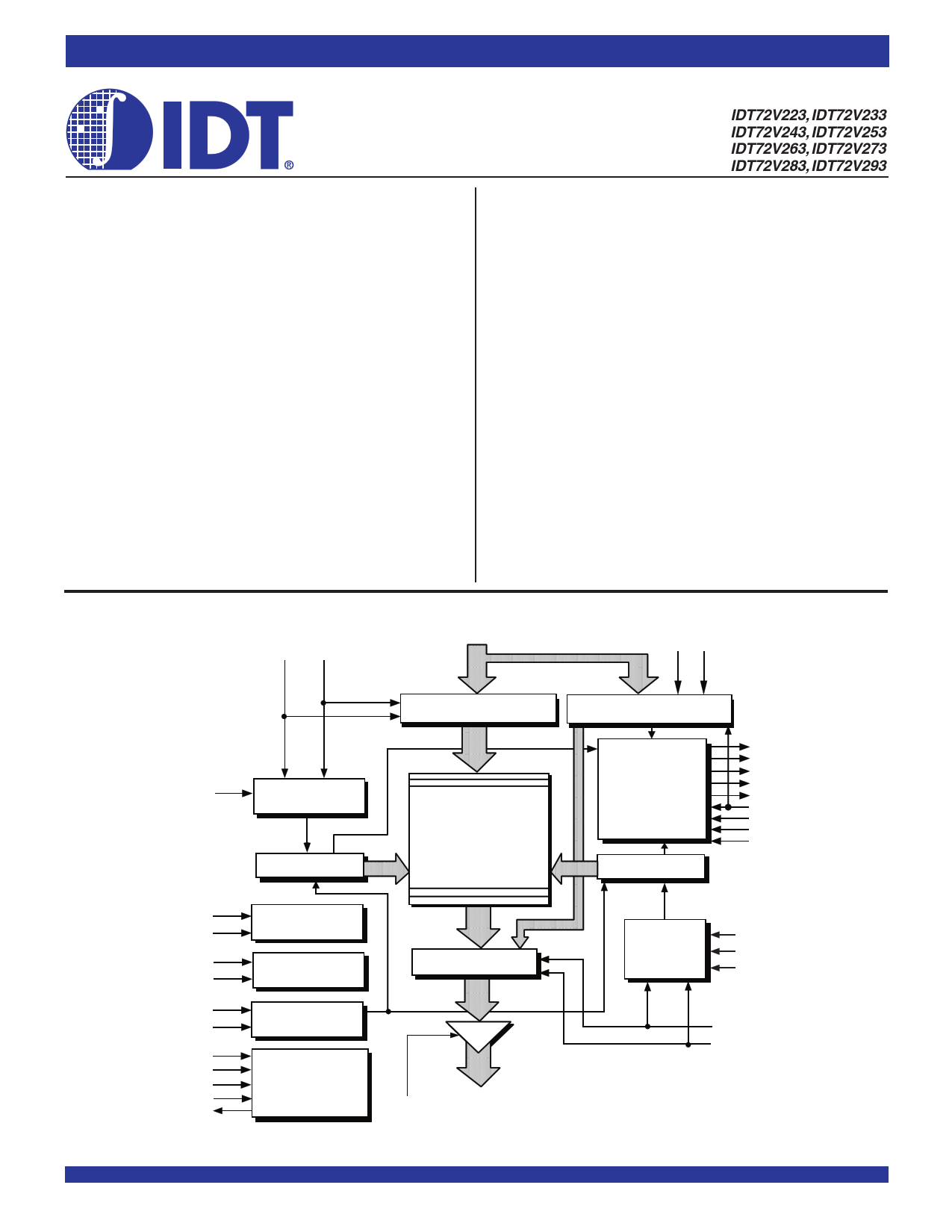
FUNCTIONAL BLOCK DIAGRAM
*Available on the
BGA package only.
*WEN WCLK/WR
D0 -Dn (x9 or x18)
LD SEN
INPUT REGISTER
OFFSET REGISTER
*ASYW
WRITE CONTROL
LOGIC
WRITE POINTER
RAM ARRAY
512 x 18 or 1,024 x 9
1,024 x 18 or 2,048 x 9
2,048 x 18 or 4,096 x 9
4,096 x 18 or 8,192 x 9
8,192 x 18 or 16,384 x 9
16,384 x 18 or 32,768 x 9
32,768 x 18 or 65,536 x 9
65,536 x 18 or 131,072 x 9
FLAG
LOGIC
READ POINTER
FF/IR
PAF
EF/OR
PAE
HF
FWFT/SI
PFM
FSEL0
FSEL1
BE CONTROL
IP LOGIC
IW BUS
OW CONFIGURATION
OUTPUT REGISTER
READ
CONTROL
LOGIC
MRS
PRS
RESET
LOGIC
TCK
*TRST
* TMS
* TDI
**TDO
*
JTAG CONTROL
(BOUNDARY SCAN)
OE
Q0 -Qn (x9 or x18)
IDT and the IDT logo are a registered trademarks of Integrated Device Technology, Inc. The SuperSync II FIFO is a trademark of Integrated Device Technology, Inc.
COMMERCIAL AND INDUSTRIAL TEMPERATURE RANGES
1
2003 Integrated Device Technology, Inc. All rights reserved. Product specifications subject to change without notice.
RT
RM
*ASYR
*RCLK/RD
REN
4666 drw01
SEPTEMBER 2003
DSC-4666/12
1 page 
IIDDTT7722VV226233//227333//228433//229533//120633//121733/238.33V/2H93IG3H.3DVEHNIGSHITDYESNUSPITEYRSSUYNPECRIISTMYNNCARIITRMONWARBRUOSWFIBFUOS FIFO
851K2xx1188,,116KKxx99//1188,,23K2Kx 9x/198/1,84,K64xK9/x189,/188K, 1x298/K18x, 196/1K8,x295/61K8, x329K/1x8,95/182,K6x49K x 9/18, 128K x 9
COMMERCIAL AND INDUSTRIAL
TEMPERATURE RANGES
to-HIGH transition of WCLK. Similarly, thePAF is asserted LOW on the LOW-
to-HIGH transition of WCLK and PAF is reset to HIGH on the LOW-to-HIGH
transition of RCLK.
If synchronous PAE/PAF configuration is selected , the PAE is asserted
and updated on the rising edge of RCLK only and not WCLK. Similarly, PAF
is asserted and updated on the rising edge of WCLK only and not RCLK. The
modedesiredisconfiguredduringmasterresetbythestateoftheProgrammable
Flag Mode (PFM) pin.
The Retransmit function allows data to be reread from the FIFO more
than once. A LOW on the RT input during a rising RCLK edge initiates a
retransmit operation by setting the read pointer to the first location of the memory
array. A zero-latency retransmit timing mode can be selected using the
Retransmit timing Mode pin (RM). During Master Reset, a LOW on RM will select
zero-latency retransmit. A HIGH on RM during Master Reset will select normal
latency.
If zero-latency retransmit operation is selected the first data word to be
retransmitted will be placed on the output register with respect to the same
RCLK edge that initiated the retransmit based on RT being LOW.
Refer to Figure 11 and 12 for Retransmit Timing with normal latency. Refer
to Figure 13 and 14 for Retransmit Timing with zero-latency.
A Big-Endian/Little-Endian data word format is provided. This function is
useful when data is written into the FIFO in long word format (x18) and read
out of the FIFO in small word (x9) format. If Big-Endian mode is selected, then
the most significant byte (word) of the long word written into the FIFO will be read
out of the FIFO first, followed by the least significant byte. If Little-Endian format
is selected, then the least significant byte of the long word written into the FIFO
will be read out first, followed by the most significant byte. The mode desired is
configured during master reset by the state of the Big-Endian (BE) pin.
The Interspersed/Non-Interspersed Parity (IP) bit function allows the user
to select the parity bit in the word loaded into the parallel port (D0-Dn) when
programming the flag offsets. If Interspersed Parity mode is selected, then the
FIFO will assume that the parity bit is located in bit position D8 during the parallel
programmingoftheflagoffsets.IfNon-InterspersedParitymodeisselected,then
D8 is assumed to be a valid bit and D16 and D17 are ignored. IP mode is selected
during Master Reset by the state of the IP input pin. This mode is relevant only
when the input width is set to x18 mode. Interspersed Parity control only has
an effect during parallel programming of the offset registers. It does not effect the
data written to and read from the FIFO.
A JTAG test port is provided, here the FIFO has fully functional Boundary
Scan feature, compliant with IEEE 1149.1 Standard Test Access Port and
Boundary Scan Architecture.
If, at any time, the FIFO is not actively performing an operation, the chip will
automatically power down. Once in the power down state, the standby supply
current consumption is minimized. Initiating any operation (by activating control
inputs) will immediately take the device out of the power down state.
The IDT72V223/72V233/72V243/72V253/72V263/72V273/72V283/
72V293are fabricated using IDT’s high speed submicron CMOS technology.
TABLE 1 — BUS-MATCHING CONFIGURATION MODES
IW OW Write Port Width
L L x18
L H x18
H L x9
H H x9
Read Port Width
x18
x9
x18
x9
5
5 Page 
IIDDTT7722VV226233//227333//228433//229533//120633//121733/238.33V/2H93IG3H.3DVEHNIGSHITDYESNUSPITEYRSSUYNPECRIISTMYNNCARIITRMONWARBRUOSWFIBFUOS FIFO
851K2xx1188,,116KKxx99//1188,,23K2Kx 9x/198/1,84,K64xK9/x189,/188K, 1x298/K18x, 196/1K8,x295/61K8, x329K/1x8,95/182,K6x49K x 9/18, 128K x 9
COMMERCIAL AND INDUSTRIAL
TEMPERATURE RANGES
AC TEST CONDITIONS
Input Pulse Levels
Input Rise/Fall Times
Input Timing Reference Levels
Output Reference Levels
Output Load for tCLK = 10ns, 15 ns
Output Load for tCLK = 6ns, 7.5ns
GND to 3.0V
3ns(1)
1.5V
1.5V
See Figure 2a
See Figure 2b & 2c
NOTE:
1. For 166Mhz and 133MHz operation input rise/fall times are 1.5ns.
ACTEST LOADS - 6ns, 7.5ns Speed Grade
1.5V
50Ω
I/O Z0 = 50Ω
4666 drw04a
Figure 2b. AC Test Load
AC TEST LOADS - 10ns, 15ns Speed Grades
D.U.T.
510Ω
3.3V
330Ω
30pF*
4666 drw04
Figure 2a. Output Load
* Includes jig and scope capacitances.
6
5
4
3
2
1
20 30 50 80 100
Capacitance (pF)
200
4666 drw04b
Figure 2c. Lumped Capacitive Load, Typical Derating
OUTPUT ENABLE & DISABLE TIMING
Output
Enable
OE
Output
Disable
Output
Normally
LOW
VCC
2
Output
Normally VCC
HIGH 2
NOTE:
1. REN is HIGH.
tOE & tOLZ
100mV
100mV
tOHZ
100mV
100mV
VIH
VIL
VCC
2
VOL
VOH
VCC
2
4666 drw04c
11
11 Page | ||
| Páginas | Total 30 Páginas | |
| PDF Descargar | [ Datasheet IDT72V223.PDF ] | |
Hoja de datos destacado
| Número de pieza | Descripción | Fabricantes |
| IDT72V221 | 3.3 VOLT CMOS SyncFIFO 256 x 9/ 512 x 9/ 1/024 x 9/ 2/048 x 9/ 4/096 x 9 and 8/192 x 9 | Integrated Device Tech |
| IDT72V223 | 3.3 VOLT HIGH-DENSITY SUPERSYNC NARROW BUS FIFO | Integrated Device Tech |
| IDT72V225 | 3.3 VOLT CMOS SyncFIFO 256 x 18/ 512 x 18/ 1/024 x 18/ 2/048 x 18/ and 4/096 x 18 | Integrated Device Tech |
| Número de pieza | Descripción | Fabricantes |
| SLA6805M | High Voltage 3 phase Motor Driver IC. |
Sanken |
| SDC1742 | 12- and 14-Bit Hybrid Synchro / Resolver-to-Digital Converters. |
Analog Devices |
|
DataSheet.es es una pagina web que funciona como un repositorio de manuales o hoja de datos de muchos de los productos más populares, |
| DataSheet.es | 2020 | Privacy Policy | Contacto | Buscar |