|
|
PDF IC43R16800 Data sheet ( Hoja de datos )
| Número de pieza | IC43R16800 | |
| Descripción | 2M x 16bit x 4 Banks DDR SDRAM | |
| Fabricantes | Integrated Circuit Solution | |
| Logotipo |  |
|
Hay una vista previa y un enlace de descarga de IC43R16800 (archivo pdf) en la parte inferior de esta página. Total 30 Páginas | ||
|
No Preview Available !
IC43R16800
Document Title
2M x 16 Bit x 4 Banks (128-MBIT) DDR SDRAM
Revision History
Revision No
0A
0B
History
Initial Draft
Mass production
Draft Date
January 20,2004
November 10,2004
Remark
The attached datasheets are provided by ICSI. Integrated Circuit Solution Inc reserve the right to change the specifications and
products. ICSI will answer to your questions about device. If you have any questions, please contact the ICSI offices.
Integrated Circuit Solution Inc.
DDR002-0B 11/10/2004
1
1 page 
IC43R16800
Signal Pin Description
Pin Type Signal Polarity
Function
CK
CK
Input Pulse
Positive The system clock input. All inputs except DQs and DMs are sampled on the rising
Edge edge of CK.
CKE
Input
Level
Active High
Activates the CK signal when high and deactivates the CK signal when low, thereby
initiates either the Power Down mode, or the Self Refresh mode.
CS Input
RAS,CAS
WE Input
CS enables the command decoder when low and disables the command decoder
Pulse Active Low when high. When the command decoder is disabled, new commands are ignored
but previous operations continue.
Pulse
Active Low
When sampled at the positive rising edge of the clock, CAS, RAS, and WE define
the command to be executed by the SDRAM.
DQS
Input/
Output
Pulse
Active on both edges for data input and output.
Active High Center aligned to input data
Edge aligned to output data
A0 - A11 Input Level
During a Bank Activate command cycle, A0-A11 defines the row address (RA0-
RA11) when sampled at the rising clock edge.
During a Read or Write command cycle, A0-A8 defines the column address (CA0-
CA8) when sampled at the rising clock edge.
_
In addition to the column address, A10(=AP) is used to invoke autoprecharge
operation at the end of the burst read or write cycle. If A10 is high, autoprecharge is
selected and BA0, BA1 defines the bank to be precharged. If A10 is low,
autoprecharge is disabled. During a Precharge command cycle, A10(=AP) is used in
conjunction with BA0 and BA1 to control which bank(s) to precharge. If A10 is high,
all four banks will be precharged simultaneously regardless of state of BA0 and BA1.
BA0,
BA1
Input Level
_ Selects which bank is to be active.
DQx Input/ Level
Output
_ Data Input/Output pins operate in the same manner as on conventional DRAMs.
DM,
LDM,
UDM
In Write mode, DM has a latency of zero and operates as a word mask by allowing
Input Pulse Active High input data to be written if it is low but blocks the write operation if is high for LDM
corresponds to data on DQ0-DQ7, UDM corresponds to data on DQ8-DQ15.
VDD,VSS Supply
Power and ground for the input buffers and the core logic.
VDDQ
VSSQ
Supply
_
VREF Input Level
_
Isolated power supply and ground for the output buffers to provide improved noise
immunity.
_ SSTL Reference Voltage for Inputs
Integrated Circuit Solution Inc.
DDR002-0B 11/10/2004
5
5 Page 
IC43R16800
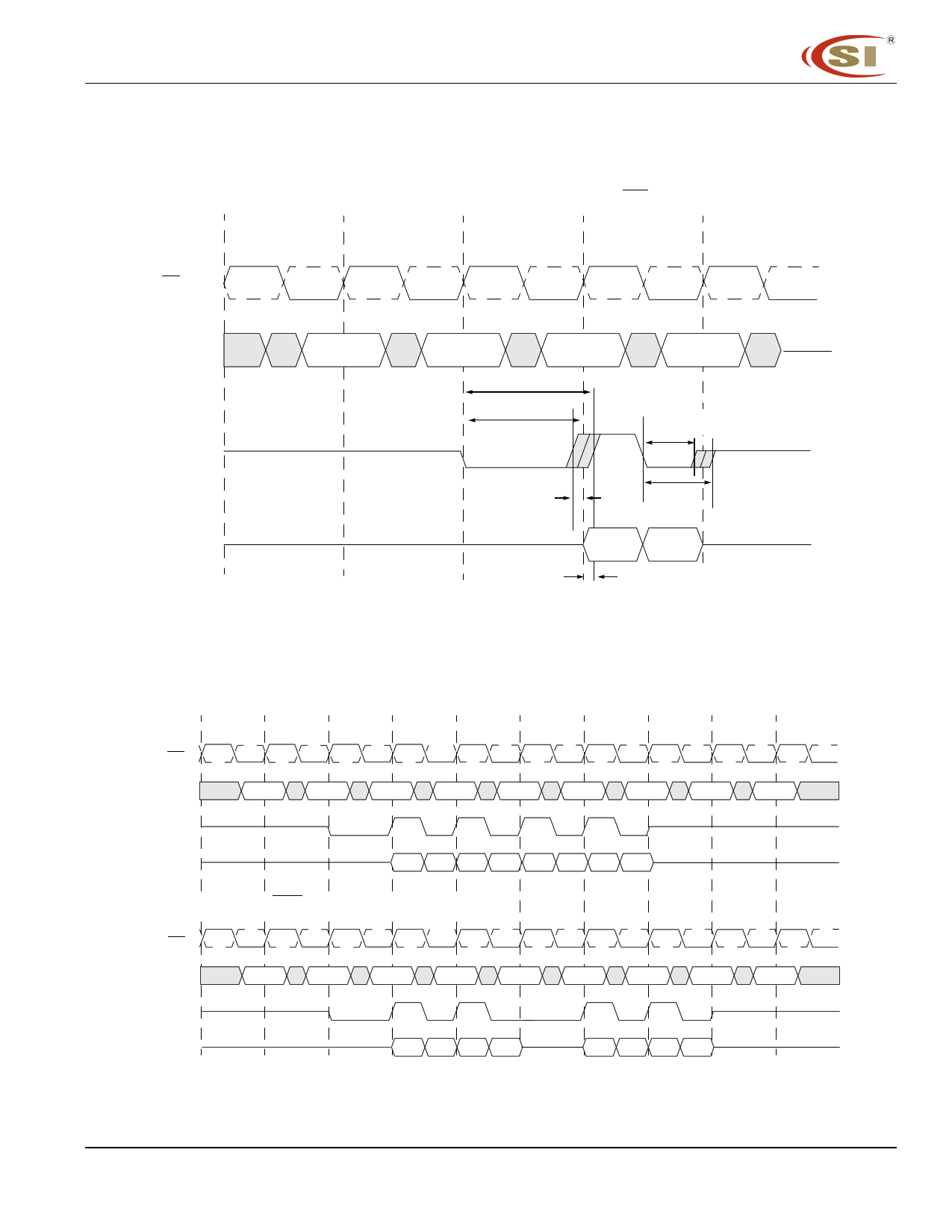
Data Strobe Preamble and Postamble Timings for DDR Read Cycles
(CAS Latency = 2; Burst Length = 2)
T0 T1 T2 T3 T4
CK, CK
Command
DQS
DQ
READ
NOP
tRPRE(min)
NOP
NOP
tRPRE(max)
tRPST(min)
tDQSQ(min)
tRPST(max)
D0 D1
tDQSQ(max)
Consecutive Burst Read Operation and Effects on the Data Strobe Preamble and Postamble
Burst Read Operation (CAS Latency = 2; Burst Length = 4)
CK, CK
Command
DQS
DQ
ReadA
NOP
ReadB
NOP
NOP
NOP
NOP
NOP
D0A D1A D2A D3A D0B D1B D2B D3B
Burst Read Operation (CAS Latency = 2; Burst Length = 4)
CK, CK
Command
DQS
DQ
ReadA
NOP
NOP
ReadB
NOP
NOP
NOP
NOP
D0A D1A D2A D3A
D0B D1B D2B D3B
NOP
NOP
Integrated Circuit Solution Inc.
DDR002-0B 11/10/2004
11
11 Page | ||
| Páginas | Total 30 Páginas | |
| PDF Descargar | [ Datasheet IC43R16800.PDF ] | |
Hoja de datos destacado
| Número de pieza | Descripción | Fabricantes |
| IC43R16800 | 2M x 16bit x 4 Banks DDR SDRAM | Integrated Circuit Solution |
| Número de pieza | Descripción | Fabricantes |
| SLA6805M | High Voltage 3 phase Motor Driver IC. |
Sanken |
| SDC1742 | 12- and 14-Bit Hybrid Synchro / Resolver-to-Digital Converters. |
Analog Devices |
|
DataSheet.es es una pagina web que funciona como un repositorio de manuales o hoja de datos de muchos de los productos más populares, |
| DataSheet.es | 2020 | Privacy Policy | Contacto | Buscar |
