|
|
|
PDF ZXFV401 Data sheet ( Hoja de datos )
| Número de pieza | ZXFV401 | |
| Descripción | SYNC SEPARATOR WITH VARIABLE FILTER | |
| Fabricantes | Zetex Semiconductors | |
| Logotipo | ||
Hay una vista previa y un enlace de descarga de ZXFV401 (archivo pdf) en la parte inferior de esta página. Total 8 Páginas | ||
|
No Preview Available !
SYNC SEPARATOR WITH VARIABLE FILTER
ZXFV401
DEVICE DESCRIPTION
The ZXFV401 provides the ability to separate out video
synchronisation signals for a wide variety of TV and CRT
display systems, standard and non-standard.
Flexibility arises from the use of just three external
resistors to adapt to each application. One resistor
controls a fully integrated internal colour carrier filter
with variable bandwidth. This filter aviods disturbance
from the colour carrier, permitting accurate threshold
slicing for timing extraction.
A second resistor controls the voltage threshold for
loss of signal detection after a time-out interval. The
third resistor controls the timing functions.
DC restoration for displays is facilitated by the Back
Porch synch output, which can be used to drive an
external curcuit to clamp the blanking voltage to a fixed
level.
ORDERING INFORMATION
Part Number
Container Increment
ZXFV401N16TA
Reel 7″
500
ZXFV401N16TC
Reel 13″
2500
FEATURES AND BENEFITS
• PAL, NTSC, SECAM, other TV systems
• Super accurate synch slice
• Variable filter for outputs: composite, horizontal,
Vertical, back porch, odd / even
• No-signal detector
• On chip sample / hold capacitors
• +5V single supply
• 4.5 mA supply current
• Default vertical output where there are no
serration pulses
• Pin compatible with industry standard part SO16N
surface mount package
APPLICATIONS
• Digital image capture
• Video input systems requiring separation of
picture timing
• Video distribution
• CCTV surveillance
• Digital multimedia
• Timing for black level clamp
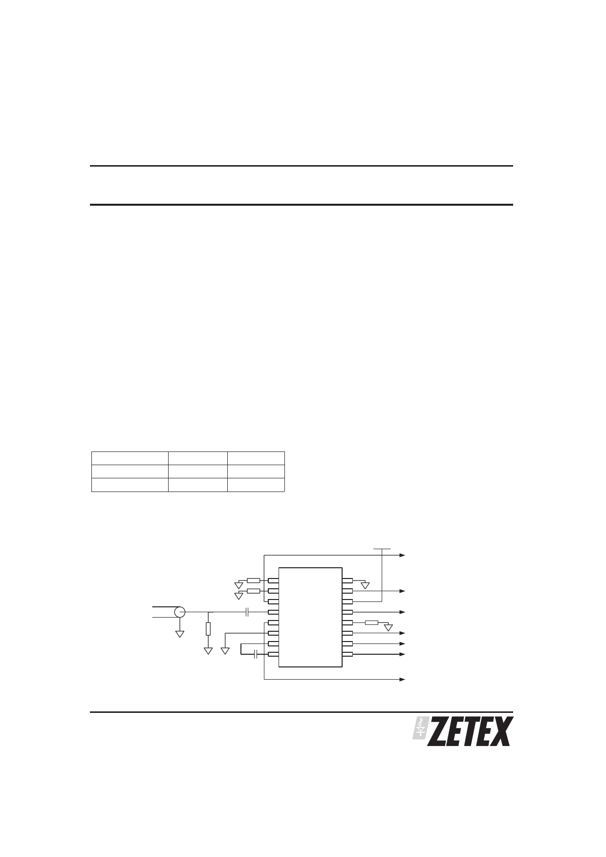
CONNECTION DIAGRAM
VIDEO INPUT
+5V
ZXFV401N16
RFILT
1 RFILT
RNOSIG
C1
2 RNOSIG
3 CSYNC
4 FILTIN
0.1uF
75R
5 VSYNC
6 0VD
C2
0.1uF
7 FILTOUT
8 FVIDIN
0VA 16
HSYNC 15
V+ 14
ODDFLD 13
RSET 12
BKPCH 11
NOSIG 10
VLEV 9
RSET
COMPOSITE SYNC
HORIZONTAL SYNC
ODD FIELD
BACK PORCH
NO SIGNAL
SYNC TIP VOLTAGE
VERTICAL SYNC
PROVISIONAL ISSUE A - FEBRUARY 2002
1
1 page 
ZXFV401
DETAIL DESCRIPTION
Introduction
This device includes all the functions required to
separate out the critical timing points of most types of
video signal. A sample-and-hold process is used to
establish accurately the 50% point of the sync pulse.
The input is also filtered to avoid the effect of the colour
carrier. The filter is coupled externally. The following
paragraphs give a simplified description of the signal
processing.
Colour Carrier Filter
This is a low-pass filter providing adjustable
attenuation of the colour carrier with low distortion of
the remaining sync pulses so as to ensure accurate
timing of the extracted logic outputs. The control is via
an external resistor RFILT connected from pin 1 to
ground. A graph shows how the bandwidth varies with
the resistor value (Graph to be provide in future issue).
Clamping Circuits
Clamping circuits are use to limit the signal swing
excursion after AC coupling at both the input to the
filter, FILTIN and the timing extractor input, FVIDIN. In
each case, the sync tip level is maintained at a value of
nominally 1.35V.
Sync Timing Extraction Circuits
The waveforms are depicted in Timing Diagrams,
Figure 1 for PAL (625 lines) and Figure 2 for NTSC (525
lines). Sample-and-hold circuits are used to obtain
time-delayed voltage values of the sync tip and the
back porch. The sample gates are controlled by a
comparator sensing the video input relative to a
threshold at a fixed offset above the sync tip clamp
level. The sampled voltages are combined in a
potential divider to derive the mean voltage (50%
amplitude), which is used as the sync pulse threshold.
A second comparator then provides CSYNC, the logic
version of the composite sync signal. This is delayed
slightly as shown in Figure 3. The time delay
comprises that of the input filter and also the smaller
delay of the comparator and logic. The timing of the
sample hold and other time parameters are all
controlled together in unison by the external resistor
RSET. A 1% resistor tolerance is recommended. The
sync tip voltage level from the sample-and-hold is
buffered and provided as an analog output, VLEV.
The vertical sync output VSYNC is derived from the
Field pulse group. Where there are short equalisation
pulses in the standard systems, these short pulses are
ignored. Essentially, a pulse width discriminator
circuit senses the first of the Field pulses, as they are
wider than those of the rest of the sequence. The
trailing edge of the first negative-going Frame Pulse
(i.e. the rising edge of the first “serration” pulse)
triggers the VSYNC output. In systems with a frame
interval with no serration pulses, a vertical sync output
is provided after a default delay as in Figure 4. Also
provided is an ODDFLD logic output, which is high
during an odd-numbered field and low during an even
one.
The horizontal sync HSYNC is a monostable output
derived from the leading edge of the composite sync.
The pulse width is about 5 µs. Also, during the Field
blanking sequence, the additional half-line pulses are
removed by a timing circuit with a pulse interval
discrimination function controlled by RSET.
The Back Porch monostable output BKPCH is initiated
from the trailing edge of the composite.sync. The
pulse is active low and the width is set according to
RSET.
Loss-of-Signal Detector
Loss of signal is indicated by a logic high level at the
output NOSIG. The decision threshold is set by an
external resistor RNOSIG connected from pin 2 to
ground. The table of connections above gives the
equation used to determine a suitable resistor value. A
waiting time of nominally 600 µs occurs before the loss
of signal is flagged.
PROVISIONAL ISSUE A - FEBRUARY 2002
5
5 Page | ||
| Páginas | Total 8 Páginas | |
| PDF Descargar | [ Datasheet ZXFV401.PDF ] | |
Hoja de datos destacado
| Número de pieza | Descripción | Fabricantes |
| ZXFV401 | SYNC SEPARATOR WITH VARIABLE FILTER | Zetex Semiconductors |
| ZXFV4089 | VIDEO AMPLIFIER WITH DC RESTORATION | Zetex Semiconductors |
| ZXFV4089N8TA | VIDEO AMPLIFIER WITH DC RESTORATION | Zetex Semiconductors |
| ZXFV4089N8TC | VIDEO AMPLIFIER WITH DC RESTORATION | Zetex Semiconductors |
| Número de pieza | Descripción | Fabricantes |
| SLA6805M | High Voltage 3 phase Motor Driver IC. |
Sanken |
| SDC1742 | 12- and 14-Bit Hybrid Synchro / Resolver-to-Digital Converters. |
Analog Devices |
|
DataSheet.es es una pagina web que funciona como un repositorio de manuales o hoja de datos de muchos de los productos más populares, |
| DataSheet.es | 2020 | Privacy Policy | Contacto | Buscar |