|
|
|
PDF ZXCW8100 Data sheet ( Hoja de datos )
| Número de pieza | ZXCW8100 | |
| Descripción | 32 BIT STEREO DIRECT DRIVE DIGITAL AUDIO AMPLIFIER | |
| Fabricantes | ETC | |
| Logotipo | ||
Hay una vista previa y un enlace de descarga de ZXCW8100 (archivo pdf) en la parte inferior de esta página. Total 24 Páginas | ||
|
No Preview Available !
Winner of the (British) Electronics Industry Design Award
for the “Best Use of Technology”
ZXCW8100S28
32 BIT STEREO DIRECT DRIVE DIGITAL AUDIO AMPLIFIER
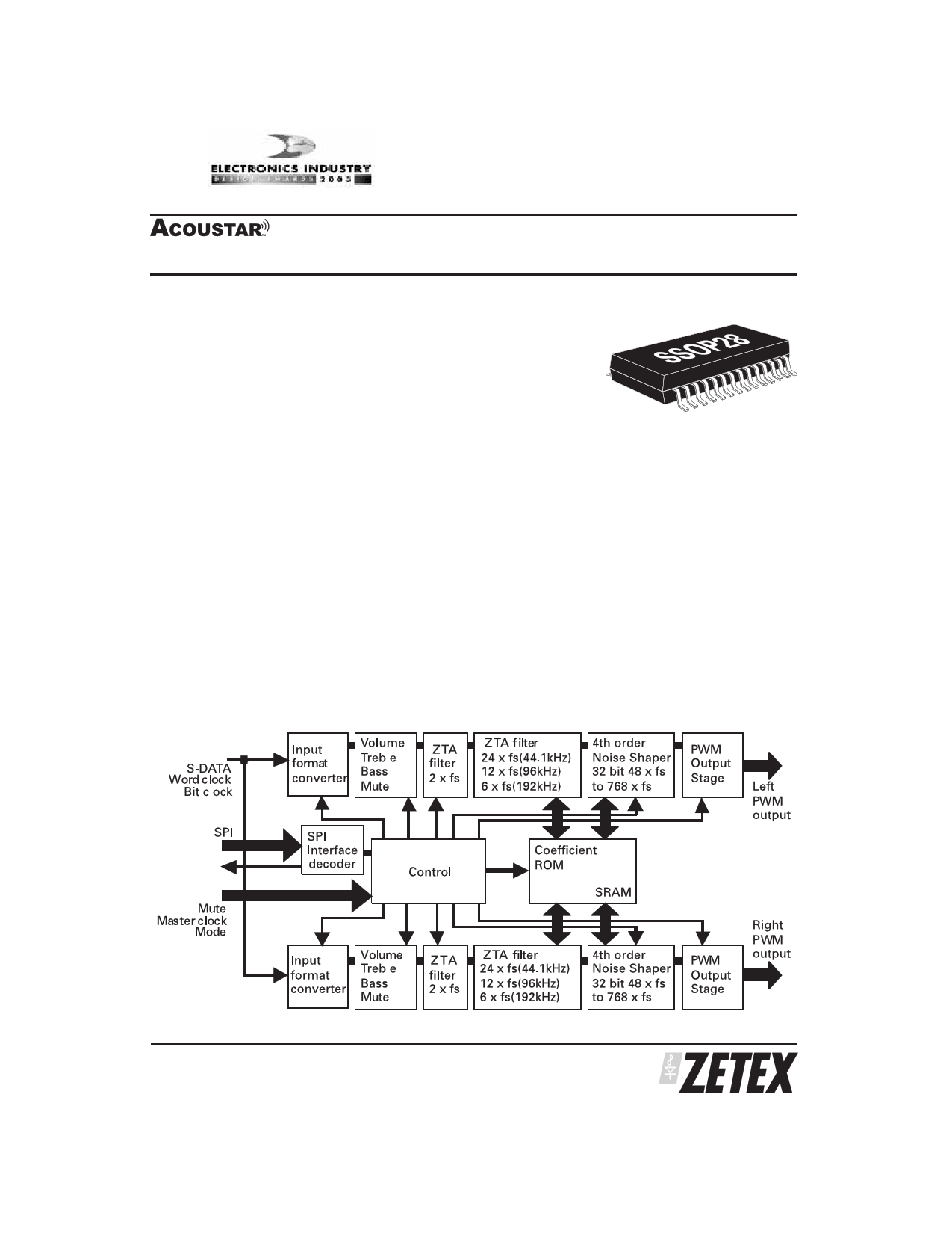
SUMMARY
The ZXCW8100S28 is part of the Acoustar™ range of new generation
digital audio power devices from Zetex. It has a level of performance not
offered by any other solution and with minimal components forms a
complete audio interface from digital audio data to the loudspeaker.
FEATURES
• Typical solution performance
THD+N (1W into 4⍀) 0.021%
Dynamic range 101dB
Noise floor -125dB
• 32 Bit conversion
• All common digital audio standards supported
• All sampling rates up to 192kHz supported
• 768 times over sampling (single speed mode)
• 48 times digital filtering (single speed mode)
• Digital de-emphasis 32,44.1,48kHz
• ATAPI mux/mute CD-ROM standard
• 3 wire SPI control interface
• ZTA filter system
• Soft mute, digital silence
• Direct drive PWM output
• Noise shaper stability up to full modulation
• Effective PWM frequency up to 2MHz
• Digital volume, mute, bass and treble control
• NOVALOAD™ for clipping control
• 28 pin SSOP package
APPLICATIONS
• 5.1 Integrated DVD amplifiers
• Home theater systems
• Mini hi-fi
• Automotive audio
• PC audio
ISSUE 3 - NOVEMBER 2003
1
SEMICONDUCTORS
1 page 
SWITCHING CHARACTERISTICS: SPI INTERFACE - WRITE
ZXCW8100S28
Symbol Parameter
SCK
tspids
tspidh
tspies
tspieh
tspiemh
SPI-CK clock frequency
SPI-DA set-up time
SPI-DA hold time
SPI-EN hold time
SPI-EN hold time
SPI-EN minimum high time
Note: 1 M-CK = Master Clock Cycles.
Conditions
SWITCHING CHARACTERISTICS: SPI INTERFACE - READ
Min
0.5
0.1
0.7
0.1
3
Typ
MCK/8
Max
40
Unit
MHz
ns
ns
ns
ns
M-CK1
Symbol Parameter
SCK
SPI-CK clock frequency
tspids
SPI-DA set-up time
tspidh
SPI-DA Data hold time
tspidov time to valid SPI-DA data out
tspies
SPI-EN hold time
tspieh
SPI-EN hold time
tspiemh SPI-EN minimum high time
Note: 1 M-CK = Master Clock Cycles.
Conditions
Load capacitance (CL) = 50pf
Min
0.5
0.1
0.7
0.1
3
ISSUE 3 - NOVEMBER 2003
5
Typ Max Unit
40 MHz
ns
ns
2.1 ns
ns
ns
M-CK1
SEMICONDUCTORS
5 Page 
ZXCW8100S28
Under normal conditions HPWM would be run at
1.058MHz as this gives the best switching
performance, however, by selecting the 2.116MHz high
frequency mode and with a high quality, high speed,
output stage it is possible to take advantage of the
better definition available through the superior noise
shaper performance. Care has to be taken however, as
an indifferent output stage can cause the higher
switching speed to give a higher level of switching
distortion that can mask the noise shaper performance
improvements.
Full details about the use of these modes is available in
the associated application document. Contact your
nearest Zetex office for full details.
Supplies
The device is provided with several power supply
connections. A nominal 3.3 volt supply is required with
the supply pairs being de-coupled separately and as
close to the device as possible.
HPWM provides a lower level of overall RF noise in the
AM band with that noise concentrated on multiples of the
switching frequency. With very careful OP stage design it
is capable of the best measured dynamic range.
RPWM is a proprietary PWM scheme that applies
different data to both sides of a conventional H bridge
output stage. The primary purpose of this is to
maximize the resolution of the internal noise shaper.
This doubles the noise shaper resolution. The other
advantage of RPWM is that the FET switching
frequency is halved. RPM therefore has two speeds of
529kHz and 1.058MHz. This lower speed does not
reduce the noise shaper performance.
The nature of RPWM also ensures that it is less
susceptible to correlated jitter on the master clock
resulting in a better signal to noise ratio with jittery
clocks.
The recommended mode of operation for new users is
HPWM with a modulation frequency of 1MHz.
Chip select
It is possible to cascade several ZXCW8100 devices for
multi-channel applications. Each chip is accessed
using the appropriate SPI enable line. Valid data for the
individual ZXCW8100 is clocked in during SPI enable
low period. SPI data and clock can be common. A
separate SPI enable line per device is required.
Mute
NOVALOAD™
The NOVALOAD™ system provides a mechanism for
overload control. It can operate in several different
ways as it acts to back off the gain of the volume or bass
blocks. Once activated there are two modes of
operation available for the user to select. With the
NOVALOAD™ Mode register bit NOVLM = 1 any
overload in the volume circuit block will result in the
gain of the volume block being reduced and if any
overload takes place in the bass circuit block then the
volume is again reduced keeping the bass boost
unaffected. With the NOVLM = 0 any overload in the
volume block will result in the gain of the volume block
being reduced, however, if any overload is present due
to bass boost the bass boost is removed completely.
When no bass clipping has occurred for a period of
time greater than that set by the limiter release rate
register (but not greater than two times that period) the
bass boost is fully restored to its previous level as
determined by the bass gain register.
The rate at which the volume is reduced in response to
clipping can be programmed through the SPI interface.
The gain reduces by 0.5dB over a selected number of
word clock periods. Typically this will be set to 0.5dB in
4 word clocks. Once the overload condition is removed
then the gain is released to increase again. This is also
programmable as 0.5dB per selected number of word
clocks. Typically this will be set to 0.5dB per 16 word
clock periods.
The release rate coming out of NOVALOAD™ is critical
to a good sound. Typically 2 seconds is suggested for
pop and rock, 4 to 8 seconds for classical.
A hard mute facility is provided for the device when
used in direct drive mode. Active low, this control will
shut off the output drive. Once released, the output will
remain disabled for approximately 0.5 seconds.
Additionally this facility can be used to provide thermal
and current overload protection.
Mode
De-emphasis
De-emphasis is activated when older audio recordings
are used in the system. These will have used
pre-emphasis to achieve noise reduction. The
de-emphasis frequency response curve is selected
versus the system sampling rate. De-emphasis only
applies in single speed mode.
The direct drive ZXCW8100 device can be operated in
different modes. In the configuration provided, the
device can operate with or without dead time
depending on the selection of output drive
characteristics. The direct drive ZXCW8100 device can
be selected though external input pins to operate with
or without dead time. It is recommended to run the
device without dead time.
ISSUE 3 - NOVEMBER 2003
11 S E M I C O N D U C T O R S
11 Page | ||
| Páginas | Total 24 Páginas | |
| PDF Descargar | [ Datasheet ZXCW8100.PDF ] | |
Hoja de datos destacado
| Número de pieza | Descripción | Fabricantes |
| ZXCW8100 | 32 BIT STEREO DIRECT DRIVE DIGITAL AUDIO AMPLIFIER | ETC |
| ZXCW8100S28 | 32 BIT STEREO DIRECT DRIVE DIGITAL AUDIO AMPLIFIER | Zetex Semiconductors |
| Número de pieza | Descripción | Fabricantes |
| SLA6805M | High Voltage 3 phase Motor Driver IC. |
Sanken |
| SDC1742 | 12- and 14-Bit Hybrid Synchro / Resolver-to-Digital Converters. |
Analog Devices |
|
DataSheet.es es una pagina web que funciona como un repositorio de manuales o hoja de datos de muchos de los productos más populares, |
| DataSheet.es | 2020 | Privacy Policy | Contacto | Buscar |