|
|
|
PDF PCM1721 Data sheet ( Hoja de datos )
| Número de pieza | PCM1721 | |
| Descripción | DIGITAL-TO-ANALOG CONVERTER WITH PROGRAMMABLE PLL | |
| Fabricantes | Burr-Brown Corporation | |
| Logotipo | ||
Hay una vista previa y un enlace de descarga de PCM1721 (archivo pdf) en la parte inferior de esta página. Total 16 Páginas | ||
|
No Preview Available !
® PCM1F479P2%O1
PCM1721
TM Stereo Audio
DIGITAL-TO-ANALOG CONVERTER
WITH PROGRAMMABLE PLL
FEATURES
q ACCEPTS 16-, 20-, OR 24-BIT INPUT DATA
q COMPLETE STEREO DAC: Includes Digital
Filter and Output Amp
q DYNAMIC RANGE: 94dB
q MULTIPLE SAMPLING FREQUENCIES:
16kHz, 22.05kHz, 24kHz
32kHz, 44.1kHz, 48kHz
64kHz, 88.2kHz, 96kHz
q PROGRAMMABLE PLL CIRCUIT:
256fS/384fS from 27MHz Master Clock
q NORMAL OR I2S DATA INPUT FORMATS
q SELECTABLE FUNCTIONS:
Soft Mute
Digital Attenuator (256 Steps)
Digital De-emphasis
q OUTPUT MODE: Left, Right, Mono, Mute
DESCRIPTION
The PCM1721 is a complete low cost stereo audio
digital-to-analog converter (DAC) with a phase-locked
loop (PLL) circuit included. The PLL derives either
256fS or 384fS system clock from an external 27MHz
reference frequency. The DAC contains a 3rd-order ∆Σ
modulator, a digital interpolation filter, and an analog
output amplifier. The PCM1721 can accept 16-, 20-, or
24-bit input data in either normal or I2S formats.
The digital filter performs an 8X interpolation func-
tion and includes selectable features such as soft mute,
digital attenuation and digital de-emphasis. The PLL
can be programmed for sampling at standard digital
audio frequencies as well as one-half and double
sampling frequencies.
The PCM1721 is ideal for applications which combine
compressed audio and video data such as DVD, DVD-
ROM, set-top boxes and MPEG sound cards.
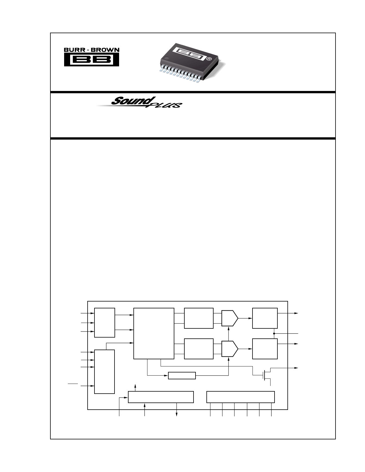
BCKIN
LRCIN
DIN
ML
MC
MD
RSTB
Serial
Input
I/F
Mode
Control
I/F
8X Oversampling
Digital Filter
with Function
Controller
Multi-level
Delta-Sigma
Modulator
Multi-level
Delta-Sigma
Modulator
256fS/384fS
BPZ-Cont.
Clock/OSC Manager and PLL
DAC
DAC
Low-pass
Filter
Low-pass
Filter
Open Drain
Power Supply
VOUTL
CAP
VOUTR
ZERO
SCKI
MCKI
SCKO
VCP PGND VCC AGND VDD DGND
International Airport Industrial Park • Mailing Address: PO Box 11400, Tucson, AZ 85734 • Street Address: 6730 S. Tucson Blvd., Tucson, AZ 85706 • Tel: (520) 746-1111 • Twx: 910-952-1111
Internet: http://www.burr-brown.com/ • FAXLine: (800) 548-6133 (US/Canada Only) • Cable: BBRCORP • Telex: 066-6491 • FAX: (520) 889-1510 • Immediate Product Info: (800) 548-6132
© 1996 Burr-Brown Corporation
PDS-11319A
PPCrintMed 1in 7U.2S.A1. August, 1996
®
1 page 
TYPICAL PERFORMANCE CURVES (CONT)
At TA = +25°C, VCC = VDD = VCP =+5V, fS = 44.1kHz, 16-bit input data, 384fS, unless otherwise noted. Measurement bandwidth is 20kHz.
DYNAMIC PERFORMANCE
THD+N vs fS
–76
–78
–80
–82
–84
–86 256fS
–88
–90 384fS
–92
–94
30 40 50 60 70 80 90 100
fS (kHz)
DYNAMIC RANGE vs fS
86
88 256fS
92
384fS
94
96
30 40 50 60 70 80 90 100
fS (kHz)
SNR vs fS
98
96 256fS
94
384fS
92
90
30 40 50 60 70 80 90 100
fS (kHz)
ICC vs fS
60
50
40
30
20
30 40 50 60 70 80 90 100
fS (kHz)
®
5 PCM1721
5 Page 
REGISTER 2 (A1 = 1, A0 = 0)
B15 B14 B13 B12 B11 B10 B9 B8 B7 B6 B5 B4 B3 B2 B1 B0
res res res res res A1 A0 PL3 PL2 PL1 PL0 IW1 IW0 OPE DEM MUTE
Register 2 is used to control soft mute, de-emphasis, opera-
tion enable, input resolution, and output format. Bit 0 is used
for soft mute: a “HIGH” level on bit 0 will cause the output
to be muted (this is ramped down in the digital domain, so
no “click” is audible). Bit 1 is used to control de-emphasis.
A “LOW” level on bit 1 disables de-emphasis, while a
“HIGH” level enables de-emphasis.
Bit 2, (OPE) is used for operational control. Table V illus-
trates the features controlled by OPE.
OPE = 1
OPE = 0
DATA INPUT
Zero
Other
Zero
Other
DAC OUTPUT
Forced to BPZ(1)
Forced to BPZ(1)
Controlled by IZD
Normal
SOFTWARE MODE
INPUT
Enabled
Enabled
Enabled
Enabled
TABLE V. Operation Enable (OPE) Function.
OPE controls the operation of the DAC: when OPE is
“LOW”, the DAC will convert all non-zero input data. If the
input data is continuously zero for 65, 536 cycles of BCKIN,
the output will be forced to zero only if IZD is “HIGH”.
When OPE is “HIGH”, the output of the DAC will be forced
to bipolar zero, irrespective of any input data.
IZD = 1
IZD = 0
DATA INPUT
Zero
Other
Zero
Other
DAC OUTPUT
Forced to BPZ(1)
Normal
Zero(2)
Normal
TABLE VI. Infinite Zero Detection (IZD) Function.
DATA INPUT
DAC OUTPUT
RSTB = “HIGH”
RSTB = “LOW”
Zero
Other
Zero
Other
Controlled by OPE and IZD
Controlled by OPE and IZD
Forced to BPZ(1)
Forced to BPZ(1)
SOFTWARE
MODE
INPUT
Enabled
Enabled
Disabled
Disabled
TABLE VII. Reset (RSTB) Function.
NOTE: (1) ∆∑ is disconnected from output amplifier. (2) ∆∑ is connected to
output amplifier.
Bits 3 (IW0) and 4 (IW1) are used to determine input word
resolution. PCM1721 can be set up for input word resolu-
tions of 16, 20, or 24 bits:
Bit 4 (IW1)
0
0
1
0
Bit 3 (IW0)
0
1
0
0
Input Resolution
16-bit Data Word
20-bit Data Word
24-bit Data Word
Reserved
Bits 5, 6, 7, and 8 (PL0:3) are used to control output format.
The output of PCM1721 can be programmed for 16 different
states, as shown in Table VIII.
PL0 PL1 PL2 PL3
0 000
0 001
0 010
0 011
0 100
0 101
0 110
0 111
1 000
1 001
1 010
1 011
1 100
1 101
1 110
1 111
Lch OUTPUT
MUTE
MUTE
MUTE
MUTE
R
R
R
R
L
L
L
L
(L + R)/2
(L + R)/2
(L + R)/2
(L + R)/2
Rch OUTPUT
MUTE
R
L
(L + R)/2
MUTE
R
L
(L + R)/2
MUTE
R
L
(L + R)/2
MUTE
R
L
(L + R)/2
NOTE
MUTE
REVERSE
STEREO
MONO
TABLE VIII. Programmable Output Format.
REGISTER 3 (A1 = 1, A0 = 1)
B15 B14 B13 B12 B11 B10 B9 B8 B7 B6 B5 B4 B3 B2 B1 B0
res res res res res A1 A0 IZD SF1 SF0 DSR1 DSR0 SYS ATC LRP I2S
Register 3 is used to control input data format and polarity,
attenuation channel control, system clock frequency, sam-
pling frequency and infinite zero detection.
Bits 0 (I2S) and 1 (LRP) are used to control the input data
format. A “LOW” on bit 0 sets the format to “Normal”
(MSB-first, right-justified Japanese format) and a “HIGH”
sets the format to I2S (Philips serial data protocol). Bit 1
(LRP) is used to select the polarity of LRCIN (sample rate
clock). When bit 1 is “LOW”, left channel data is assumed
when LRCIN is in a “HIGH” phase and right channel data
is assumed when LRCIN is in a “LOW” phase. When bit
1 is “HIGH”, the polarity assumption is reversed.
Bit 2 (ATC) is used for controlling the attenuator. When
bit 2 is “HIGH”, the attenuation data loaded in program
Register 0 is used for both left and right channels. When
bit 2 is “LOW”, the attenuation data for each register is
applied separately to left and right channels.
Bit 3 (SYS) is the system clock selection. When bit 3 is
“LOW”, the system clock frequency is set to 384fS. When
bit 3 is “HIGH”, the system clock frequency is set to 256fS.
Bits 4 (DSR0) and 5 (DSR1) are used to control multiples
of the sampling rate:
DSR1
0
0
1
1
DSR0
0
1
0
1
Normal
Double
One-half
Reserved
Multiple
32/44.1/48kHz
64/88.2/96kHz
16/22.05/24kHz
Not Defined
®
11 PCM1721
11 Page | ||
| Páginas | Total 16 Páginas | |
| PDF Descargar | [ Datasheet PCM1721.PDF ] | |
Hoja de datos destacado
| Número de pieza | Descripción | Fabricantes |
| PCM1720 | Stereo Audio DIGITAL-TO-ANALOG CONVERTER MPEG2/AC-3 COMPATIBLE | Burr-Brown Corporation |
| PCM1720 | SoundPlus Stereo Audio Digital-To-Analog Converter MPEG2/AC-3 Compatible | Texas Instruments |
| PCM1721 | DIGITAL-TO-ANALOG CONVERTER WITH PROGRAMMABLE PLL | Burr-Brown Corporation |
| PCM1723 | Stereo Audio DIGITAL-TO-ANALOG CONVERTER WITH PROGRAMMABLE PLL | Burr-Brown Corporation |
| Número de pieza | Descripción | Fabricantes |
| SLA6805M | High Voltage 3 phase Motor Driver IC. |
Sanken |
| SDC1742 | 12- and 14-Bit Hybrid Synchro / Resolver-to-Digital Converters. |
Analog Devices |
|
DataSheet.es es una pagina web que funciona como un repositorio de manuales o hoja de datos de muchos de los productos más populares, |
| DataSheet.es | 2020 | Privacy Policy | Contacto | Buscar |