|
|
|
PDF X1227 Data sheet ( Hoja de datos )
| Número de pieza | X1227 | |
| Descripción | Real Time Clock/Calendar/CPU Supervisor with EEPROM | |
| Fabricantes | Xicor | |
| Logotipo | ||
Hay una vista previa y un enlace de descarga de X1227 (archivo pdf) en la parte inferior de esta página. Total 28 Páginas | ||
|
No Preview Available !
New Features
Repetitive Alarms &
Temperature Compensation
4K (512 x 8)
X1227
2-Wire™ RTC
Real Time Clock/Calendar/CPU Supervisor with EEPROM
FEATURES
• Real Time Clock/Calendar
— Tracks time in Hours, Minutes, and Seconds
— Day of the Week, Day, Month, and Year
• 2 Polled Alarms (Non-volatile)
— Settable on the Second, Minute, Hour, Day of the
Week, Day, or Month
— Repeat Mode (periodic interrupts)
• Oscillator Compensation on chip
— Internal feedback resistor and compensation
capacitors
— 64 position Digitally Controlled Trim Capacitor
— 6 digital frequency adjustment settings to ±30ppm
• CPU Supervisor Functions
— Power On Reset, Low Voltage Sense
— Watchdog Timer (SW Selectable: 0.25s, 0.75s,
1.75s, off)
• Battery Switch or Super Cap Input
• 4K x 8 Bits of EEPROM
— 64-Byte Page Write Mode
— 8 modes of Block Lock™ Protection
— Single Byte Write Capability
• High Reliability
— Data Retention: 100 years
— Endurance: 100,000 cycles per byte
• 2-Wire™ Interface interoperable with I2C*
— 400kHz data transfer rate
• Low Power CMOS
— 1.25µA Operating Current (Typical)
• Small Package Options
— 8-Lead SOIC and 8-Lead TSSOP
APPLICATIONS
• Utility Meters
• HVAC Equipment
• Audio / Video Components
• Set Top Box / Television
• Modems
• Network Routers, Hubs, Switches, Bridges
• Cellular Infrastructure Equipment
• Fixed Broadband Wireless Equipment
• Pagers / PDA
• POS Equipment
• Test Meters / Fixtures
• Office Automation (Copiers, Fax)
• Home Appliances
• Computer Products
• Other Industrial / Medical / Automotive
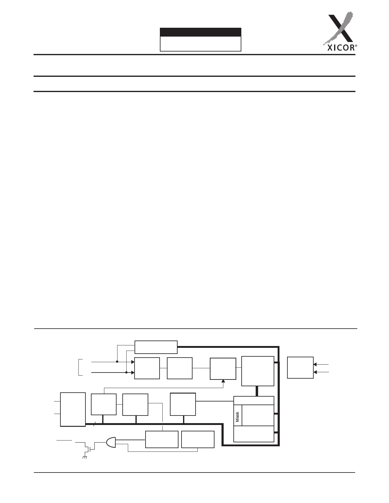
DESCRIPTION
The X1227 device is a Real Time Clock with clock/
calendar, two polled alarms with integrated 512x8
EEPROM, oscillator compensation, CPU Supervisor
(POR/LVS and WDT) and battery backup switch.
The oscillator uses an external, low-cost 32.768kHz
crystal. All compensation and trim components are
integrated on the chip. This eliminates several external
discrete components and a trim capacitor, saving
board area and component cost.
BLOCK DIAGRAM
32.768kHz
X1
X2
OSC
Compensation
Oscillator
Frequency 1Hz
Divider
Timer
Calendar
Logic
Time
Keeping
Registers
(SRAM)
Battery
Switch
Circuitry
VCC
VBACK
SCL
SDA
Serial
Interface
Decoder
RESET
Control
Decode
Logic
8
Control/
Registers
(EEPROM)
Status
Registers
(SRAM)
Alarm
Watchdog
Timer
Low Voltage
Reset
Compare
Alarm Regs
(EEPROM)
4K
EEPROM
ARRAY
*I2C is a Trademark of Philips.
REV 1.1.20 1/13/03
www.xicor.com
Characteristics subject to change without notice. 1 of 28
1 page 
X1227
When there is a match, an alarm flag is set. The occur-
rence of an alarm can be determined by polling the
AL0 and AL1 bits or by enabling the IRQ output, using
it as hardware flag.
The alarm enable bits are located in the MSB of the
particular register. When all enable bits are set to ‘0’,
there are no alarms.
STATUS REGISTER (SR)
The Status Register is located in the CCR Memory
Map at address 003Fh. This is a volatile register only
and is used to control the WEL and RWEL write
enable latches, read two power status and two alarm
bits. This register is separate from both the array and
the Clock/Control Registers (CCR).
– The user can set the X1227 to alarm every Wednes-
day at 8:00 AM by setting the EDWn*, the EHRn*
and EMNn* enable bits to ‘1’ and setting the DWAn*,
HRAn* and MNAn* Alarm registers to 8:00 AM
Wednesday.
– A daily alarm for 9:30PM results when the EHRn*
and EMNn* enable bits are set to ‘1’ and the HRAn*
and MNAn* registers are set to 9:30 PM.
*n = 0 for Alarm 0: N = 1 for Alarm 1
REAL TIME CLOCK REGISTERS
Clock/Calendar Registers (SC, MN, HR, DT, MO,
YR)
These registers depict BCD representations of the
time. As such, SC (Seconds) and MN (Minutes) range
from 00 to 59, HR (Hour) is 1 to 12 with an AM or PM
indicator (H21 bit) or 0 to 23 (with MIL=1), DT (Date) is
1 to 31, MO (Month) is 1 to 12, YR (Year) is 0 to 99.
Date of the Week Register (DW)
This register provides a Day of the Week status and
uses three bits DY2 to DY0 to represent the seven
days of the week. The counter advances in the cycle
0-1-2-3-4-5-6-0-1-2-… The assignment of a numerical
value to a specific day of the week is arbitrary and may
be decided by the system software designer. The
default value is defined as ‘0’.
24 Hour Time
If the MIL bit of the HR register is 1, the RTC uses a
24-hour format. If the MIL bit is 0, the RTC uses a 12-
hour format and H21 bit functions as an AM/PM indi-
cator with a ‘1’ representing PM. The clock defaults to
standard time with H21=0.
Leap Years
Leap years add the day February 29 and are defined
as those years that are divisible by 4. Years divisible by
100 are not leap years, unless they are also divisible
by 400. This means that the year 2000 is a leap year,
the year 2100 is not. The X1227 does not correct for
the leap year in the year 2100.
Table 2. Status Register (SR)
Addr 7 6 5 4 3 2
10
003Fh BAT AL1 AL0 0 0 RWEL WEL RTCF
Default 0 0 0 0 0 0
01
BAT: Battery Supply—Volatile
This bit set to “1” indicates that the device is operating
from VBACK, not VCC. It is a read-only bit and is set/
reset by hardware (X1227 internally). Once the device
begins operating from VCC, the device sets this bit to
“0”.
AL1, AL0: Alarm bits—Volatile
These bits announce if either alarm 0 or alarm 1 match
the real time clock. If there is a match, the respective
bit is set to ‘1’. The falling edge of the last data bit in a
SR Read operation resets the flags. Note: Only the AL
bits that are set when an SR read starts will be reset.
An alarm bit that is set by an alarm occurring during an
SR read operation will remain set after the read opera-
tion is complete.
RWEL: Register Write Enable Latch—Volatile
This bit is a volatile latch that powers up in the LOW
(disabled) state. The RWEL bit must be set to “1” prior
to any writes to the Clock/Control Registers. Writes to
RWEL bit do not cause a nonvolatile write cycle, so the
device is ready for the next operation immediately after
the stop condition. A write to the CCR requires both
the RWEL and WEL bits to be set in a specific
sequence.
WEL: Write Enable Latch—Volatile
The WEL bit controls the access to the CCR and
memory array during a write operation. This bit is a
volatile latch that powers up in the LOW (disabled)
state. While the WEL bit is LOW, writes to the CCR or
any array address will be ignored (no acknowledge will
be issued after the Data Byte). The WEL bit is set by
writing a “1” to the WEL bit and zeroes to the other bits
of the Status Register. Once set, WEL remains set
until either reset to 0 (by writing a “0” to the WEL bit
and zeroes to the other bits of the Status Register) or
REV 1.1.20 1/13/03
www.xicor.com
Characteristics subject to change without notice. 5 of 28
5 Page 
X1227
Figure 7. Valid Data Changes on the SDA Bus
SCL
SDA
Data Stable
Data Change
Data Stable
Figure 8. Valid Start and Stop Conditions
SCL
SDA
Start
Figure 9. Acknowledge Response From Receiver
SCL from
Master
Data Output
from Transmitter
1
Data Output
from Receiver
Start
Stop
89
Acknowledge
DEVICE ADDRESSING
Following a start condition, the master must output a
Slave Address Byte. The first four bits of the Slave
Address Byte specify access to either the EEPROM
array or to the CCR. Slave bits ‘1010’ access the
EEPROM array. Slave bits ‘1101’ access the CCR.
When shipped from the factory, EEPROM array is
UNDEFINED, and should be programmed by the cus-
tomer to a known state.
Bit 3 through Bit 1 of the slave byte specify the device
select bits. These are set to ‘111’.
The last bit of the Slave Address Byte defines the oper-
ation to be performed. When this R/W bit is a one, then
a read operation is selected. A zero selects a write
operation. Refer to Figure 10.
After loading the entire Slave Address Byte from the
SDA bus, the X1227 compares the device identifier
and device select bits with ‘1010111’ or ‘1101111’.
Upon a correct compare, the device outputs an
acknowledge on the SDA line.
Following the Slave Byte is a two byte word address.
The word address is either supplied by the master
device or obtained from an internal counter. On power
up the internal address counter is set to address 0h, so
a current address read of the EEPROM array starts at
address 0. When required, as part of a random read,
the master must supply the 2 Word Address Bytes as
shown in Figure 10.
In a random read operation, the slave byte in the
“dummy write” portion must match the slave byte in the
“read” section. That is if the random read is from the
array the slave byte must be 1010111x in both
instances. Similarly, for a random read of the Clock/
Control Registers, the slave byte must be 1101111x in
both places.
REV 1.1.20 1/13/03
www.xicor.com
Characteristics subject to change without notice. 11 of 28
11 Page | ||
| Páginas | Total 28 Páginas | |
| PDF Descargar | [ Datasheet X1227.PDF ] | |
Hoja de datos destacado
| Número de pieza | Descripción | Fabricantes |
| X1226 | Real Time Clock/Calendar with EEPROM | Xicor |
| X1226 | Real Time Clock/Calendar | Intersil Corporation |
| X1227 | Real Time Clock/Calendar/CPU Supervisor with EEPROM | Xicor |
| X1227 | RTC Real TimeClock/Calendar/ CPU Supervisor | Intersil Corporation |
| Número de pieza | Descripción | Fabricantes |
| SLA6805M | High Voltage 3 phase Motor Driver IC. |
Sanken |
| SDC1742 | 12- and 14-Bit Hybrid Synchro / Resolver-to-Digital Converters. |
Analog Devices |
|
DataSheet.es es una pagina web que funciona como un repositorio de manuales o hoja de datos de muchos de los productos más populares, |
| DataSheet.es | 2020 | Privacy Policy | Contacto | Buscar |