|
|
|
PDF X1226 Data sheet ( Hoja de datos )
| Número de pieza | X1226 | |
| Descripción | Real Time Clock/Calendar with EEPROM | |
| Fabricantes | Xicor | |
| Logotipo | ||
Hay una vista previa y un enlace de descarga de X1226 (archivo pdf) en la parte inferior de esta página. Total 24 Páginas | ||
|
No Preview Available !
4K (512 x 8)
New Features
Repetitive Alarms &
Temperature Compensation
X1226
Real Time Clock/Calendar with EEPROM
2-Wire™ RTC
FEATURES
• Real Time Clock/Calendar
—Tracks time in Hours, Minutes, and Seconds
—Day of the Week, Day, Month, and Year
• 2 Polled Alarms (Non-volatile)
—Settable on the Second, Minute, Hour, Day of
the Week, Day, or Month
—Repeat Mode (periodic interrupts)
• Oscillator Compensation on chip
—Internal feedback resistor and compensation
capacitors
—64 position Digitally Controlled Trim Capacitor
—6 digital frequency adjustment settings to
±30ppm
• Battery Switch or Super Cap Input
• 512 x 8 Bits of EEPROM
—64-Byte Page Write Mode
—8 modes of Block Lock™ Protection
—Single Byte Write Capability
• High Reliability
—Data Retention: 100 years
—Endurance: 100,000 cycles per byte
• 2-Wire™ Interface interoperable with I2C*
—400kHz data transfer rate
• Frequency Output (SW Selectable: Off, 1Hz,
4096Hz or 32.768kHz)
• Low Power CMOS
—1.25µA Operating Current (Typical)
• Small Package Options
—8-Lead SOIC and 8-Lead TSSOP
APPLICATIONS
• Utility Meters
• HVAC Equipment
• Audio / Video Components
• Set Top Box / Television
• Modems
• Network Routers, Hubs, Switches, Bridges
• Cellular Infrastructure Equipment
• Fixed Broadband Wireless Equipment
• Pagers / PDA
• POS Equipment
• Test Meters / Fixtures
• Office Automation (Copiers, Fax)
• Home Appliances
• Computer Products
• Other Industrial / Medical / Automotive
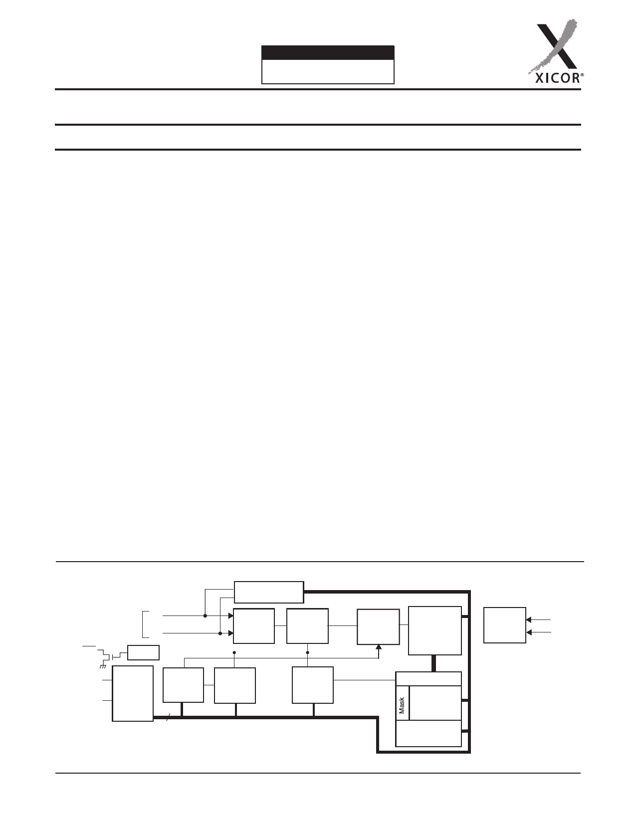
DESCRIPTION
The X1226 device is a Real Time Clock with clock/
calendar, two polled alarms with integrated 512x8
EEPROM, oscillator compensation, and battery
backup switch.
The oscillator uses an external, low-cost 32.768kHz
crystal. All compensation and trim components are
integrated on the chip. This eliminates several external
discrete components and a trim capacitor, saving
board area and component cost.
BLOCK DIAGRAM
32.768kHz
X1
X2
PHZ/IRQ
Select
SCL
SDA
Serial
Interface
Decoder
Control
Decode
Logic
8
*I2C is a Trademark of Philips.
REV 1.1.24 1/13/03
OSC
Compensation
Oscillator
Frequency 1Hz
Divider
Timer
Calendar
Logic
Time
Keeping
Registers
(SRAM)
Control/
Registers
(EEPROM)
Status
Registers
(SRAM)
Alarm
Compare
Alarm Regs
(EEPROM)
4K
EEPROM
ARRAY
Battery
Switch
Circuitry
VCC
VBACK
www.xicor.com
Characteristics subject to change without notice. 1 of 24
1 page 
X1226
ALARM REGISTERS
There are two alarm registers whose contents mimic the
contents of the RTC register, but add enable bits and
exclude the 24 hour time selection bit. The enable bits
specify which registers to use in the comparison between
the Alarm and Real Time Registers. For example:
– Setting the Enable Month bit (EMOn*) bit in combi-
nation with other enable bits and a specific alarm
time, the user can establish an alarm that triggers at
the same time once a year.
*n = 0 for Alarm 0: N = 1 for Alarm 1
When there is a match, an alarm flag is set. The occur-
rence of an alarm can be determined by polling the
AL0 and AL1 bits or by enabling the IRQ output, using
it as hardware flag.
The alarm enable bits are located in the MSB of the
particular register. When all enable bits are set to ‘0’,
there are no alarms.
indicator with a ‘1’ representing PM. The clock defaults
to standard time with H21=0.
Leap Years
Leap years add the day February 29 and are defined
as those years that are divisible by 4. Years divisible by
100 are not leap years, unless they are also divisible
by 400. This means that the year 2000 is a leap year,
the year 2100 is not. The X1226 does not correct for
the leap year in the year 2100.
STATUS REGISTER (SR)
The Status Register is located in the CCR memory
map at address 003Fh. This is a volatile register only
and is used to control the WEL and RWEL write
enable latches, read power status and two alarm bits.
This register is separate from both the array and the
Clock/Control Registers (CCR).
Table 2. Status Register (SR)
– The user can set the X1226 to alarm every Wednes-
day at 8:00 AM by setting the EDWn*, the EHRn*
and EMNn* enable bits to ‘1’ and setting the DWAn*,
HRAn* and MNAn* Alarm registers to 8:00 AM
Wednesday.
– A daily alarm for 9:30PM results when the EHRn*
and EMNn* enable bits are set to ‘1’ and the HRAn*
and MNAn* registers are set to 9:30 PM.
*n = 0 for Alarm 0: N = 1 for Alarm 1
REAL TIME CLOCK REGISTERS
Addr 7 6 5 4 3 2
10
003Fh BAT AL1 AL0 0 0 RWEL WEL RTCF
Default 0 0 0 0 0 0
01
BAT: Battery Supply—Volatile
This bit set to “1” indicates that the device is operating
from VBACK, not VCC. It is a read-only bit and is set/
reset by hardware (X1226 internally). Once the device
begins operating from VCC, the device sets this bit to
“0”.
Clock/Calendar Registers (SC, MN, HR, DT, MO, YR)
These registers depict BCD representations of the
time. As such, SC (Seconds) and MN (Minutes) range
from 00 to 59, HR (Hour) is 1 to 12 with an AM or PM
indicator (H21 bit) or 0 to 23 (with MIL=1), DT (Date) is
1 to 31, MO (Month) is 1 to 12, YR (Year) is 0 to 99.
Date of the Week Register (DW)
This register provides a Day of the Week status and
uses three bits DY2 to DY0 to represent the seven
days of the week. The counter advances in the cycle
0-1-2-3-4-5-6-0-1-2-… The assignment of a numerical
value to a specific day of the week is arbitrary and may
be decided by the system software designer. The
default value is defined as ‘0’.
24 Hour Time
If the MIL bit of the HR register is 1, the RTC uses a
24-hour format. If the MIL bit is 0, the RTC uses a 12-
hour format and H21 bit functions as an AM/PM
AL1, AL0: Alarm bits—Volatile
These bits announce if either alarm 0 or alarm 1 match
the real time clock. If there is a match, the respective
bit is set to ‘1’. The falling edge of the last data bit in a
SR Read operation resets the flags. Note: Only the AL
bits that are set when an SR read starts will be reset.
An alarm bit that is set by an alarm occurring during an
SR read operation will remain set after the read opera-
tion is complete.
RWEL: Register Write Enable Latch—Volatile
This bit is a volatile latch that powers up in the LOW
(disabled) state. The RWEL bit must be set to “1” prior
to any writes to the Clock/Control Registers. Writes to
RWEL bit do not cause a nonvolatile write cycle, so the
device is ready for the next operation immediately after
the stop condition. A write to the CCR requires both
the RWEL and WEL bits to be set in a specific
sequence.
REV 1.1.24 1/13/03
www.xicor.com
Characteristics subject to change without notice. 5 of 24
5 Page 
X1226
A write to a protected block of memory is ignored, but
will still receive an acknowledge. At the end of the write
command, the X1226 will not initiate an internal write
cycle, and will continue to ACK commands.
Page Write
The X1226 has a page write operation. It is initiated in
the same manner as the byte write operation; but
instead of terminating the write cycle after the first data
byte is transferred, the master can transmit up to 63
more bytes to the memory array and up to 7 more
bytes to the clock/control registers. (Note: Prior to writ-
ing to the CCR, the master must write a 02h, then 06h
to the status register in two preceding operations to
enable the write operation. See “Writing to the Clock/
Control Registers.”
After the receipt of each byte, the X1226 responds with
an acknowledge, and the address is internally incre-
mented by one. When the counter reaches the end of
the page, it “rolls over” and goes back to the first
address on the same page. This means that the mas-
ter can write 64 bytes to a memory array page or 8
bytes to a CCR section starting at any location on that
page. For example, if the master begins writing at loca-
tion 60 of the memory and loads 30 bytes, then the first
23 bytes are written to addresses 40 through 63, and
the last 7 bytes are written to columns 0 through 6.
Afterwards, the address counter would point to location
7 on the page that was just written. If the master sup-
plies more than the maximum bytes in a page, then the
previously loaded data is over written by the new data,
one byte at a time. Refer to Figure 8.
The master terminates the Data Byte loading by issu-
ing a stop condition, which causes the X1226 to begin
the nonvolatile write cycle. As with the byte write oper-
ation, all inputs are disabled until completion of the
internal write cycle. Refer to Figure 9 for the address,
acknowledge, and data transfer sequence.
Stops and Write Modes
Stop conditions that terminate write operations must
be sent by the master after sending at least 1 full data
byte and it’s associated ACK signal. If a stop is issued
in the middle of a data byte, or before 1 full data byte +
ACK is sent, then the X1226 resets itself without per-
forming the write. The contents of the array are not
affected.
Figure 9. Page Write Sequence
Signals from
the Master
SDA Bus
Signals from
the Slave
S
t
a
r
Slave
t Address
Word
Address 1
Word
Address 0
1 11 10 000 00 0 0
AA
CC
KK
1 ≤ n ≤ 64 for EEPROM array
1 ≤ n ≤ 8 for CCR
Data
(1)
Data
(n)
S
t
o
p
AA
CC
KK
REV 1.1.24 1/13/03
www.xicor.com
Characteristics subject to change without notice. 11 of 24
11 Page | ||
| Páginas | Total 24 Páginas | |
| PDF Descargar | [ Datasheet X1226.PDF ] | |
Hoja de datos destacado
| Número de pieza | Descripción | Fabricantes |
| X1226 | Real Time Clock/Calendar with EEPROM | Xicor |
| X1226 | Real Time Clock/Calendar | Intersil Corporation |
| X1227 | Real Time Clock/Calendar/CPU Supervisor with EEPROM | Xicor |
| X1227 | RTC Real TimeClock/Calendar/ CPU Supervisor | Intersil Corporation |
| Número de pieza | Descripción | Fabricantes |
| SLA6805M | High Voltage 3 phase Motor Driver IC. |
Sanken |
| SDC1742 | 12- and 14-Bit Hybrid Synchro / Resolver-to-Digital Converters. |
Analog Devices |
|
DataSheet.es es una pagina web que funciona como un repositorio de manuales o hoja de datos de muchos de los productos más populares, |
| DataSheet.es | 2020 | Privacy Policy | Contacto | Buscar |