|
|
|
PDF WM0834 Data sheet ( Hoja de datos )
| Número de pieza | WM0834 | |
| Descripción | 8-Bit ADCs with Serial Interface and Configurable Input Multiplexer | |
| Fabricantes | Wolfson Microelectronics plc | |
| Logotipo | ||
Hay una vista previa y un enlace de descarga de WM0834 (archivo pdf) en la parte inferior de esta página. Total 16 Páginas | ||
|
No Preview Available !
WM0834, WM0838
Production Data
Sept 1996 Rev 2.0
8-Bit ADCs with Serial Interface and
Configurable Input Multiplexer
Description
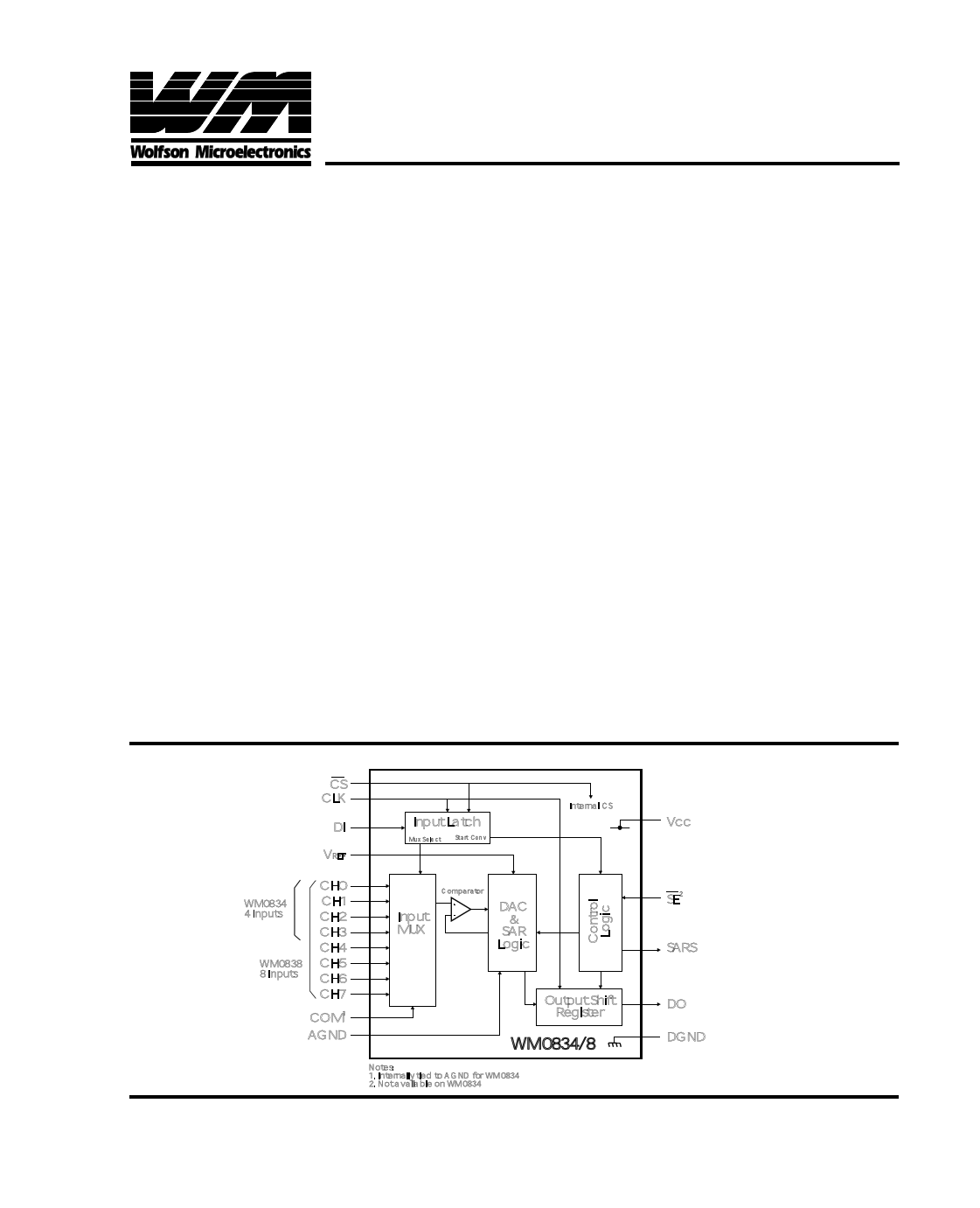
WM0834 and WM0838 are 8-bit analogue to digital
converters (ADC) with configurable 4-input and 8-input
multiplexers respectively and a serial I/O interface.
Assignment of the multiplexer inputs is configured before
each conversion via the serial data input to give single-ended
or differential operation for the selected inputs. A mixture of
input configurations can be used in the same application.
WM0838 also has a pseudo-differential configuration where
all 8 inputs can be refered to a common input at an arbitrary
voltage.
Serial communcation with WM0834/8 is via Data In (DI) and
Data Out (DO) wires under the control of clock and chip
select inputs. A high output at the SARS pin indicates when
the conversion is in progress. To initiate a conversion chip
enable is held low and data is input to DI on the rising edge
of the clock, comprising, a start bit, and bits to set up the
input configuration and polarity. After a half clock cycle delay
conversion results appear at DO on the falling edge of the
clock, MSB first, concurrently with A-D conversion. This is
followed by the results LSB first, indicated by the falling edge
of SARS. WM0838 has a shift enable (SE) input used to
control the LSB first output on DO.
WM0834/8 operate on 5V and 3.3V supply voltages and
are available in small outline and DIP packages for com-
mercial (0 to 70OC) and industrial (-40 to 85OC) tempera-
ture ranges.
Features
• Functionally Equivalent to National Semiconduc-
tor ADC0834 and ADC0838 without the Internal
Zener Regulator Network
• 4-input (WM0834) or 8-input (WM0838) MUX
options
• Reference input operates ratiometrically or with
a fixed reference
• Input range 0 to Vcc with Vcc Reference
• 5V and 3.3V variants
• Total Unadjusted Error: ± 1 LSB
• 8-bit resolution
• Low Power
• 32 µs conversion time at fclock = 250 kHz
• Serial I/O interface
• WM0834 packages: 14 pin SO & DIP
WM0838 packages: 20 pin wide-body SO & DIP
Applications
• Embedding with remote sensors
• Equipment health monitoring
• Automotive
• Industrial control
Block Diagram
CS
CLK
DI
VREF
Input Latch
Mux Select Start Conv
Internal CS
Vcc
WM0834
4 Inputs
WM0838
8 Inputs
CH0
CH1
CH2
CH3
CH4
CH5
CH6
CH7
COM1
AGND
Input
MUX
Comparator
DAC
&
SAR
Logic
Output Shift
Register
WM0834/8
Notes:
1. Internally tied to AGND for WM0834
2. Not available on WM0834
SE2
SARS
DO
DGND
Production Data data sheets contain final
specifications current on publication date. Supply
of products conforms to Wolfson Microelectronics
standard terms and conditions.
Wolfson Microelectronics
Lutton Court, Bernard Terrace, Edinburgh EH8 9NX, UK
Tel: +44 (0) 131 667 9386 Fax: +44 (0) 131 667 5176
email: [email protected]
www: http://www.wolfson.co.uk
© 1996 Wolfson Microelectronics
1 page 
WM0834, WM0838
Electrical Characteristics (3.3V)
VCC = 3.3V, fCLK = 250 KHz, TA = TMIN to TMAX , tr = tf = 20ns, unless otherwise stated.
PARAMETER
SYMBOL
TEST CONDITIONS
MIN
Digital Inputs
High level output voltage
VOH VCC = 3.0 V, IOH = -360 mA
2.4
VCC = 3.0V, IOH = -10 mA
2.8
Low level output voltage
VOL VCC =3.0V, IOH = 1.6 mA
High level input current
IIH VIH = 3.6V
Low level input current
IIL VIL = 0 V
High level output (source) IOH VOH = 0 V, TA = 25oC
6.5
current
Low level output (sink) current IOL
VOL = VCC, TA = 25oC
8
High impedance-state
IOZ VO = 3.3 V, TA = 25oC
output current (DO)
VO = 0 V, TA = 25oC
Input capacitance
Ci
Output capacitance
Co
Converter and Multiplexer
Total unadjusted error
TUE VREF = 3.3 V. (note 7)
Differential Linearity
(note 8)
8
Supply voltage variation error Vs(error) VCC = 3.0 V to 3.6 V
Common mode error
Differential mode
Common mode input voltage VICR (note 9)
GND-0.05
range
VCC+0.05
Standby input leakage
II(stdby) On-channel VI =3.3 V at ON ch.
current (note 10)
Off-channel VI = 0 V at OFF ch.
On-channel VI = 0 V at ON ch.
Off-channel VI =3.3V at OFF ch
Conversion time
tconv Excluding MUX addressing time
TYP
0.005
-0.005
15
16
0.01
-0.01
5
5
±1/16
±1/16
Reference Inputs
Input resistance to
reference ladder
Total device
Supply current
Timing Parameters
Setup time, CS low or
data valid before clock
Hold time, data valid after
clock
Propagation delay time,
output data after clock
Output disable time, DO
after CS
Ri(REF)
1.3
ICC
tsu 350
th 90
MSB data first. CL = 100 pF
tpd LSB data first. CL = 100 pF
tdis CL = 10 pF, RL = 10 kΩ
CL = 100 pF, RL = 2 kΩ
2.4
0.2
MAX
0.4
1
-1
3
-3
±1
±1/4
±1/4
1
-1
-1
1
8
5.9
0.75
500
200
80
250
UNIT
V
V
V
µA
µA
mA
mA
µA
µA
pF
pF
LSB
Bits
LSB
LSB
V
µA
µA
µA
µA
clock
periods
kΩ
mA
ns
ns
ns
ns
ns
ns
Wolfson Microelectronics
5
5 Page 
Functional Description (continued)
WM0834, WM0838
WM0834 MUX Addressing
MUX Address
Channel Number
SGL/DIF
ODD/EVEN
Select bit
0
1
2
Differential MUX Mode (Between adjacent pairs of points)
00
0 +-
00
1
+
01
0 -+
01
1
-
Single Ended MUX Mode (between selected input(s) and AGND)
10
0+
10
1
+
11
0
+
11
1
3
-
+
+
Note: Analogue common input 'COM' used with single ended mode is internally tied to AGND
All internal registers are cleared when CS is high. To
initiate another conversion, CS must make a high to low
transition and MUX address assignments input to DI.
The DI inpit and DO output can be tied together and
controlled via a bidirectional processor I/O bit line.
Reference Input
The analogue input voltage range Vmax to Vmin for
differential and pseudo-differential input is defined by the
voltage applied to the reference input with respect to
AGND.
WM0834/8 can be used in ratiometric appliacations or
those requiring absolute accuracy. A ratiometric input is
typically the Vcc and is the same supply used to power
analogue input circuitry and sensors. In such systems
under a given input condition, the same code will be
output with variations in supply voltage, because the same
ratio change occurs in both the analogue and reference
input to the A/D. When used in applications requiring ab-
solute accuracy, a suitable time and temperature stable
voltage reference source should be used.
Analogue Inputs
While sampling the analogue inputs, short spikes of
current enter a "+" input and flow out of the corresponding
"-" input at the clock edges during conversion. This
current does not cause errors as it decays rapidly and the
internal comparator is strobed at the end of a clock period.
Care should be exercised if bypass capacitors are used at
the inputs as an apparant offset error can be caused by the
capacitor averaging the input current and developing a volt-
age across the source resistance. Bypass capacitors should
not be used with a source resistance greater than 1kΩ.
In considering error sources, input leakage current will also
cause a voltage drop across the source resistance and
hence, high impedance sources should be buffered.
In differential mode, there is a 1/2 clock period interval
between sampling the "+" and the "-" inputs. If there is a
change in common mode voltage during this interval, an
errorcould notionally result.
For a sinusoidal common mode signal, the error is given
by:
The voltage source used to drive the reference input should
be capable of driving the 2.4kΩ typical of the SAR resistor
ladder. The maximum input voltage to the reference input
is the Vcc supply voltage. The minimum can be as least
as low as 1V to allow for direct conversion of sensor
outputs with output voltage ranges less than 5V.
VERROR = VPEAK (2πfCM) (1/(2fCLK))
Where
VPEAK = peak common mode voltage
fCM = common mode signal frequency
fCLK = clock frequency
Wolfson Microelectronics
11
11 Page | ||
| Páginas | Total 16 Páginas | |
| PDF Descargar | [ Datasheet WM0834.PDF ] | |
Hoja de datos destacado
| Número de pieza | Descripción | Fabricantes |
| WM0831 | 8-Bit ADCs with Serial Interface and Differential or Dual Inputs | Wolfson Microelectronics plc |
| WM0832 | 8-Bit ADCs with Serial Interface and Differential or Dual Inputs | Wolfson Microelectronics plc |
| WM0834 | 8-Bit ADCs with Serial Interface and Configurable Input Multiplexer | Wolfson Microelectronics plc |
| WM0838 | 8-Bit ADCs with Serial Interface and Configurable Input Multiplexer | Wolfson Microelectronics plc |
| Número de pieza | Descripción | Fabricantes |
| SLA6805M | High Voltage 3 phase Motor Driver IC. |
Sanken |
| SDC1742 | 12- and 14-Bit Hybrid Synchro / Resolver-to-Digital Converters. |
Analog Devices |
|
DataSheet.es es una pagina web que funciona como un repositorio de manuales o hoja de datos de muchos de los productos más populares, |
| DataSheet.es | 2020 | Privacy Policy | Contacto | Buscar |