|
|
PDF W49V002AQ Data sheet ( Hoja de datos )
| Número de pieza | W49V002AQ | |
| Descripción | 256K x 8 CMOS FLASH MEMORY WITH LPC INTERFACE | |
| Fabricantes | Winbond | |
| Logotipo |  |
|
Hay una vista previa y un enlace de descarga de W49V002AQ (archivo pdf) en la parte inferior de esta página. Total 32 Páginas | ||
|
No Preview Available !
Preliminary W49V002A
256K x 8 CMOS FLASH MEMORY
WITH LPC INTERFACE
GENERAL DESCRIPTION
The W49V002A is a 2-megabit, 3.3-volt only CMOS flash memory organized as 256K × 8 bits. The
device can be programmed and erased in-system with a standard 3.3V power supply. A 12-volt VPP is
not required. The unique cell architecture of the W49V002A results in fast program/erase operations with
extremely low current consumption. This device can operate at two modes, Programmer bus interface
mode and LPC bus interface mode. As in the Programmer interface mode, it acts like the traditional
flash but with a multiplexed address inputs. But in the LPC interface mode, this device complies with the
Intel LPC specification 1.0. The device can also be programmed and erased using standard EPROM
programmers.
FEATURES
•Single 3.3-volt operations:
− 3.3-volt Read
− 3.3-volt Erase
− 3.3-volt Program
• Fast Program operation:
− Byte-by-Byte programming: 50 µS (typ.)
• Fast Erase operation: 150 mS (typ.)
• Endurance: 10K cycles (typ.)
• Twenty-year data retention
• Hardware data protection
− #TBL & #WP serve as hardware protection
• One 16K bytes Boot Block with lockout
protection
• Two 8K bytes Parameter Blocks
• Four Main Memory Blocks (with 32K bytes, 64K
bytes, 64K bytes, 64K bytes each)
• Low power consumption
− Active current: 25 mA (typ.)
− Standby current: 20 µA (typ.)
• Automatic program and erase timing with
internal VPP generation
• End of program or erase detection
− Toggle bit
− Data polling
• Latched address and data
• TTL compatible I/O
• Available packages: 32L PLCC and 32L
STSOP
Publication Release Date: April 2001
- 1 - Revision A1
1 page 
Preliminary W49V002A
Memory Address Map
There are 8M bytes space reserved for BIOS Addressing. The ROM will respond to 256K byte pages
whenever the memory address rang is within the top 4M bytes and bottom 128K bytes.
The 32bit address space is as below:
Block
Address Range
4M Byte BIOS ROM
FFFF,FFFFh:FFC0,0000h
128K Byte BIOS ROM 000F,FFFFh:000E,0000h
Registers
FFBC,0100h
General Purpose Inputs Register
This register reads the GPI[4:0] pins on the W49V002A.This is a pass-through register which can read
via memory address FFBC0100(hex). Since it is pass-through register, there is no default value.
Bit Function
7-5 Reserved
4 Read GPI4 pin status
3 Read GPI3 pin status
2 Read GPI2 pin status
1 Read GPI1 pin status
0 Read GPI0 pin status
Product Identification
The product ID operation outputs the manufacturer code and device code. Programming equipment
automatically matches the device with its proper erase and programming algorithms.
The manufacturer and device codes can be accessed by software operation. In the software access
mode, a six-byte (or JEDEC 3-byte) command sequence can be used to access the product ID. A read
from address 0000(hex) outputs the manufacturer code, DA(hex). A read from address 0001(hex) outputs
the device code, B0(hex).” The product ID operation can be terminated by a three-byte command
sequence or an alternate one-byte command sequence (see Command Definition table).
Publication Release Date: April 2001
- 5 - Revision A1
5 Page 
Preliminary W49V002A
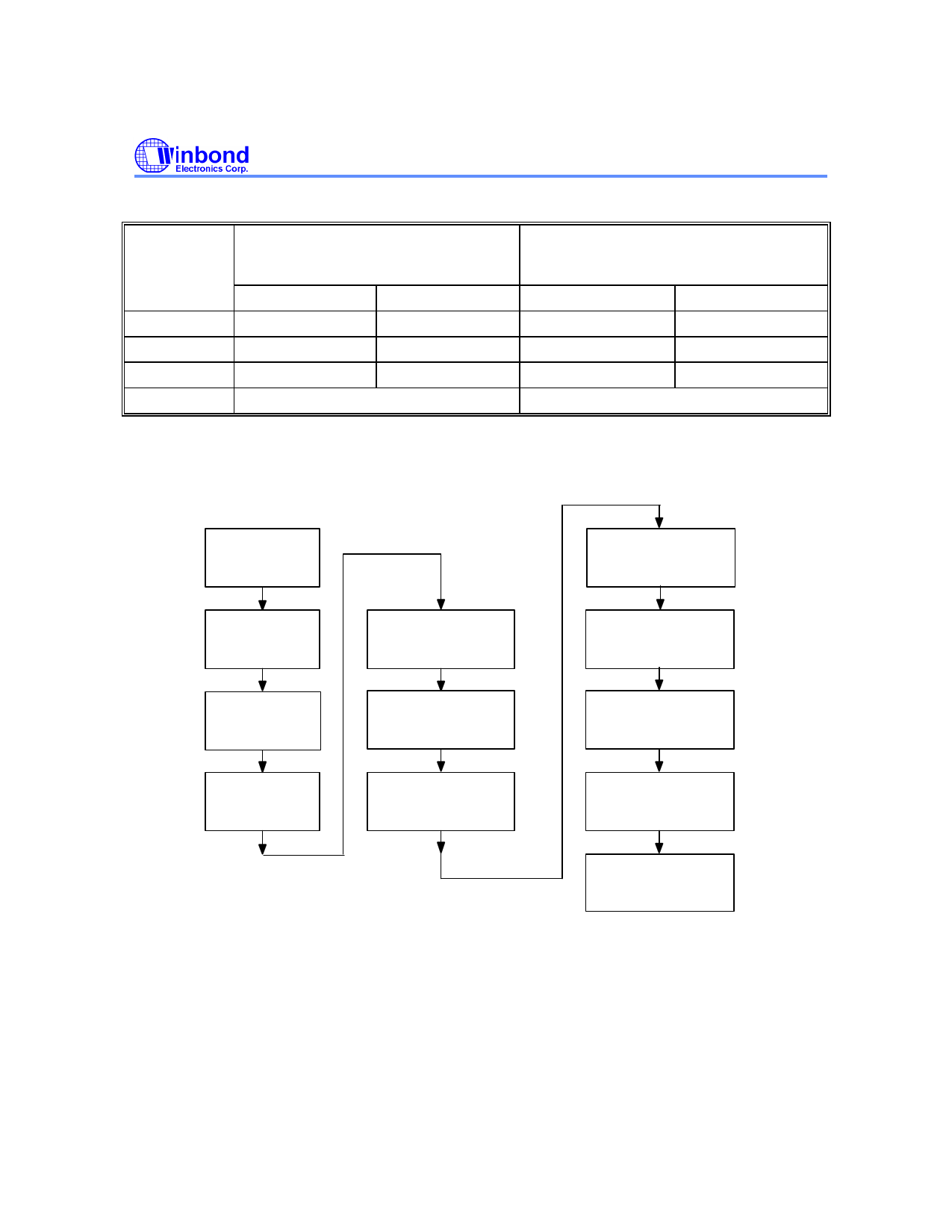
Command Codes for Product Identification and Boot Block Lockout Detection
BYTE
SEQUENCE
1 Write
2 Write
3 Write
SOFTWARE PRODUCT IDENTIFICATION /
BOOT BLOCK LOCKOUT DETECTION
ENTRY
ADDRESS
DATA
5555
AA
2AAA
55
5555
90
Pause 10µS
SOFTWARE PRODUCT IDENTIFICATION /
BOOT BLOCK LOCKOUT DETECTION
EXIT (6)
ADDRESS
DATA
5555H
AAH
2AAAH
55H
5555H
F0H
Pause 10µS
Software Product Identification and Boot Block Lockout Detection Acquisition Flow
Product
Identification
Entry (1)
Load data AA
to
address 5555
Product
Identification
and Boot Block
Lockout Detection
Mode (3)
Product
Identification Exit(6)
Load data AA
to
address 5555
Load data 55
to
address 2AAA
Read address = 00000
data = DA
(2)
Load data 55
to
address 2AAA
Load data 90
to
address 5555
Read address = 00001
data = B0
(2)
Load data F0
to
address 5555
Pause 10µ S
(4)
Read address = 00002
DQ0 of data outputs = 1/0
Pause 10µ S
Normal Mode
(5)
Notes for software product identification/boot block lockout detection:
(1) Data Format: DQ7−DQ0 (Hex); Address Format: A14−A0 (Hex)
(2) A1−A17 = VIL; manufacture code is read for A0 = VIL; device code is read for A0 = VIH.
(3) The device does not remain in identification and boot block lockout detection mode if power down.
(4) If the DQ0 of output data is "1," the boot block programming lockout feature is activated; if the DQ0 of output data "0," the lockout feature
is inactivated and the block can be programmed.
(5) The device returns to standard operation mode.
(6) Optional 1-write cycle (write F0 hex at XXXX address) can be used to exit the product identification/boot block lockout detection.
- 11 -
Publication Release Date: April 2001
Revision A1
11 Page | ||
| Páginas | Total 32 Páginas | |
| PDF Descargar | [ Datasheet W49V002AQ.PDF ] | |
Hoja de datos destacado
| Número de pieza | Descripción | Fabricantes |
| W49V002A | 256K x 8 CMOS FLASH MEMORY WITH LPC INTERFACE | Winbond |
| W49V002AP | 256K x 8 CMOS FLASH MEMORY WITH LPC INTERFACE | Winbond |
| W49V002AQ | 256K x 8 CMOS FLASH MEMORY WITH LPC INTERFACE | Winbond |
| Número de pieza | Descripción | Fabricantes |
| SLA6805M | High Voltage 3 phase Motor Driver IC. |
Sanken |
| SDC1742 | 12- and 14-Bit Hybrid Synchro / Resolver-to-Digital Converters. |
Analog Devices |
|
DataSheet.es es una pagina web que funciona como un repositorio de manuales o hoja de datos de muchos de los productos más populares, |
| DataSheet.es | 2020 | Privacy Policy | Contacto | Buscar |
