|
|
|
PDF W195B Data sheet ( Hoja de datos )
| Número de pieza | W195B | |
| Descripción | Frequency Generator for Integrated Core Logic | |
| Fabricantes | Cypress Semiconductor | |
| Logotipo | ||
Hay una vista previa y un enlace de descarga de W195B (archivo pdf) en la parte inferior de esta página. Total 13 Páginas | ||
|
No Preview Available !
PRELIMINARY
W195B
Frequency Generator for Integrated Core Logic
Features
• Maximized EMI suppression using Cypress’s Spread
Spectrum Technology
• Low jitter and tightly controlled clock skew
• Highly integrated device providing clocks required for
CPU, core logic, and SDRAM
• Two copies of CPU clocks
• Nine copies of SDRAM clocks
• Eight copies of PCI clock
• One copy of synchronous APIC clock
• Two copies of 66-MHz outputs
• Two copies of 48-MHz outputs
• One copy of selectable 24- or 48-MHz clock
• One copy of double strength 14.31818-MHz reference
clock
• Power-down control
• I2C interface for turning off unused clocks
Key Specifications
CPU, SDRAM Outputs Cycle-to-Cycle Jitter: ............. 250 ps
APIC, 48MHz, 3V66, PCI Outputs
Cycle-to-Cycle Jitter: .................................................. 500 ps
CPU, 3V66 Output Skew: ........................................... 175 ps
SDRAM, APIC, 48MHz Output Skew: ........................ 250 ps
PCI Output Skew: ........................................................500 ps
CPU to SDRAM Skew (@100 MHz): ..................4.5 to 5.5 ns
CPU to 3V66 Skew (@ 66 MHz): ....................... 7.0 to 8.0 ns
3V66 to PCI Skew (3V66 lead):.......................... 1.5 to 3.5 ns
PCI to APIC Skew: ....................................................± 0.5 ns
Table 1. Frequency Selections
FS3 FS2 FS1 FS0 CPU SDRAM 3V66 PCI APIC
1 1 1 1 133.6 133.6 66.8 33.4 16.7
1110
Reserved
1 1 0 1 100.2 100.2 66.8 33.4 16.7
1 1 0 0 66.8 100.2 66.8 33.4 16.7
1 0 1 1 105 105 70 35 17.5
1 0 1 0 110 110 73.3 36.7 18.3
1 0 0 1 114 114 76 38 19
1 0 0 0 119 119 79.3 39.7 19.8
0 1 1 1 124 124 82.7 41.3 20.7
0 1 1 0 129 129 64.5 32.3 16.1
0 1 0 1 95
95 63.3 31.7 15.8
0 1 0 0 138 138 69 34.5 17.3
0 0 1 1 150 150 75 37.5 18.8
0 0 1 0 75 113 75 37.5 18.8
0 0 0 1 90 90 60 30 15
0 0 0 0 83.3 125 83.3 41.7 20.8
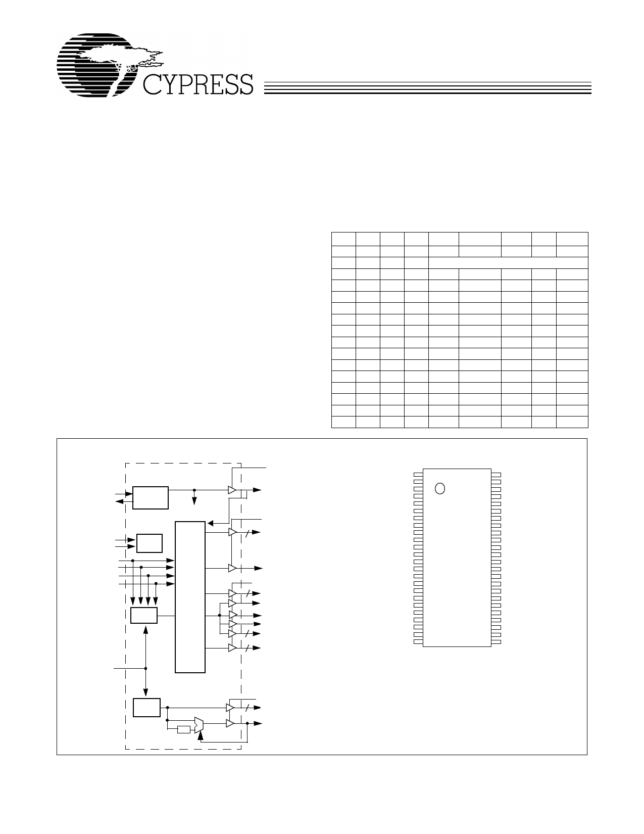
Block Diagram
X1 XTAL
X2 OSC
PLL REF FREQ
SDATA
SCLK
FS3*
FS2*
FS1*
FS0*
I2C
Logic
Divider,
Delay,
and
Phase
Control
Logic
PLL 1
PWRDWN#
PLL2
/2
VDDQ3
REF2X/FS3*
VDDQ2
CPU0:1
2
APIC
VDDQ3
3V66_0:1
2
PCI0/FS0*
PCI1/FS1*
PCI2/FS2*
PCI3:7
5
SDRAM0:8
9
VDDQ3
48MHz_0:1
2
SI0/24_48#MHz*
[1]
Pin Configuration
REF2x/FS3*
VDDQ3
X1
X2
GND
VDDQ3
3V66_0
3V66_1
GND
FS0*/PCI0
FS1^/PCI1
FS2*/PCI2
GND
PCI3
PCI4
VDDQ3
PCI5
PCI6
PCI7
GND
48MHz_0
48MHz_1
SI0/24_48#MHz*
VDDQ3
1
2
3
4
5
6
7
8
9
10
11
12
13
14
15
16
17
18
19
20
21
22
23
24
48 VDDQ2
47 APIC
46 VDDQ2
45 CPU0
44 CPU1
43 GND
42 VDDQ3
41 SDRAM0
40 SDRAM1
39 SDRAM2
38 GND
37 SDRAM3
36 SDRAM4
35 SDRAM5
34 VDDQ3
33 SDRAM6
32 SDRAM7
31 SDRAM8
30 GND
29 PWRDWN#*
28 SCLK
27 VDDQ3
26 GND
25 SDATA
Note:
1. Internal 250K pull-up or pull down resistors present on inputs
marked with * or ^ respectively. Design should not rely solely on
internal pull-up or pull down resistor to set I/O pins HIGH or LOW
respectively.
Cypress Semiconductor Corporation • 3901 North First Street • San Jose • CA 95134 • 408-943-2600
October 13, 1999, rev. **
1 page 
PRELIMINARY
W195B
Spread Spectrum Generator
The device generates a clock that is frequency modulated in
order to increase the bandwidth that it occupies. By increasing
the bandwidth of the fundamental and its harmonics, the am-
plitudes of the radiated electromagnetic emissions are re-
duced. This effect is depicted in Figure 5.
As shown in Figure 5, a harmonic of a modulated clock has a
much lower amplitude than that of an unmodulated signal. The
reduction in amplitude is dependent on the harmonic number
and the frequency deviation or spread. The equation for the
reduction is
dB = 6.5 + 9*log10(P) + 9*log10(F)
Where P is the percentage of deviation and F is the frequency
in MHz where the reduction is measured.
The output clock is modulated with a waveform depicted in
Figure 6. This waveform, as discussed in “Spread Spectrum
Clock Generation for the Reduction of Radiated Emissions” by
Bush, Fessler, and Hardin produces the maximum reduction
in the amplitude of radiated electromagnetic emissions. The
deviation selected for this chip is –0.5% of the selected fre-
quency. Figure 6 details the Cypress spreading pattern.
Cypress does offer options with more spread and greater EMI
reduction. Contact your local Sales representative for details
on these devices.
EMI Reduction
Spread
Spectrum
Enabled
Non-
Spread
Spectrum
MAX.
Figure 5. Typical Clock and SSFTG Comparison
MIN.
Figure 6. Typical Modulation Profile
5
5 Page 
PRELIMINARY
W195B
AC Electrical Characteristics
TA = 0°C to +70°C, VDDQ3 = 3.3V±5%, VDDQ2= 2.5V±5%
fXTL = 14.31818 MHz
Spread Spectrum function turned off
Parameter
Description
TPeriod
THIGH
TLOW
TRISE
TFALL
Host/CPUCLK Period
Host/CPUCLK High Time
Host/CPUCLK Low Time
Host/CPUCLK Rise Time
Host/CPUCLK Fall Time
66.6-MHz Host
Min.
Max.
15.0
15.5
5.2 N/A
5.0 N/A
0.4 1.6
0.4 1.6
100-MHz Host
Min.
Max.
10.0 10.5
3.0 N/A
2.8 N/A
0.4 1.6
0.4 1.6
Unit
ns
ns
ns
ns
ns
Notes
10
13
14
TPeriod
THIGH
TLOW
TRISE
TFALL
SDRAM CLK Period
SDRAM CLK High Time
SDRAM CLK Low Time
SDRAM CLK Rise Time
SDRAM CLK Fall Time
10.0
3.0
2.8
0.4
0.4
10.5
N/A
N/A
1.6
1.6
10.0
3.0
2.8
0.4
0.4
10.5
N/A
N/A
1.6
1.6
ns 10
ns 13
ns 14
ns
ns
TPeriod
THIGH
TLOW
TRISE
TFALL
APIC CLK Period
APIC CLK High Time
APIC CLK Low Time
APIC CLK Rise Time
APIC CLK Fall Time
60.0
25.5
25.3
0.4
0.4
64.0
N/A
N/A
1.6
1.6
60.0
25.5
25.3
0.4
0.4
64.0
N/A
N/A
1.6
1.6
ns 10
ns 13
ns 14
ns
ns
TPeriod
THIGH
TLOW
TRISE
TFALL
3V66 CLK Period
3V66 CLK High Time
3V66 CLK Low Time
3V66 CLK Rise Time
3V66 CLK Fall Time
15.0
5.25
5.05
0.5
0.5
16.0
N/A
N/A
2.0
2.0
15.0
5.25
5.05
0.5
0.5
16.0
N/A
N/A
2.0
2.0
ns 10, 12
ns 13
ns 14
ns
ns
TPeriod
THIGH
TLOW
TRISE
TFALL
PCI CLK Period
PCI CLK High Time
PCI CLK Low Time
PCI CLK Rise Time
PCI CLK Fall Time
30.0 N/A 30.0 N/A
12.0 N/A 12.0 N/A
12.0 N/A 12.0 N/A
0.5 2.0 0.5 2.0
0.5 2.0 0.5 2.0
ns 10, 11
ns 13
ns 14
ns
ns
tpZL, tpZH Output Enable Delay (All outputs)
1.0 10.0 1.0 10.0 ns
tpLZ, tpZH Output Disable Delay (All outputs)
1.0 10.0 1.0 10.0 ns
tstable
All Clock Stabilization from Power-Up
3 3 ms
Notes:
10. Period, jitter, offset, and skew measured on rising edge at 1.25 for 2.5V clocks and at 1.5V for 3.3V clocks.
11. THIGH is measured at 2.0V for 2.5V outputs, 2.4V for 3.3V outputs.
12. TLOW is measured at 0.4V for all outputs.
13. The time specified is measured from when VDDQ3 achieves its nominal operating level (typical condition VDDQ3 = 3.3V) until the frequency output is stable and
operating within specification.
14. TRISE and TFALL are measured as a transition through the threshold region Vol = 0.4V and Voh = 2.0V (1 mA) JEDEC specification.
11
11 Page | ||
| Páginas | Total 13 Páginas | |
| PDF Descargar | [ Datasheet W195B.PDF ] | |
Hoja de datos destacado
| Número de pieza | Descripción | Fabricantes |
| W195B | Frequency Generator for Integrated Core Logic | Cypress Semiconductor |
| Número de pieza | Descripción | Fabricantes |
| SLA6805M | High Voltage 3 phase Motor Driver IC. |
Sanken |
| SDC1742 | 12- and 14-Bit Hybrid Synchro / Resolver-to-Digital Converters. |
Analog Devices |
|
DataSheet.es es una pagina web que funciona como un repositorio de manuales o hoja de datos de muchos de los productos más populares, |
| DataSheet.es | 2020 | Privacy Policy | Contacto | Buscar |