|
|
|
PDF W166 Data sheet ( Hoja de datos )
| Número de pieza | W166 | |
| Descripción | Spread Spectrum Frequency Timing Generator | |
| Fabricantes | Cypress Semiconductor | |
| Logotipo | ||
Hay una vista previa y un enlace de descarga de W166 (archivo pdf) en la parte inferior de esta página. Total 7 Páginas | ||
|
No Preview Available !
W166
Spread Spectrum Frequency Timing Generator
Features
• Maximized EMI suppression using Cypress’s Spread
Spectrum technology
• Generates a spread spectrum copy of the provided
input
• Selectable spreading characteristics
• Integrated loop filter components
• Operates with a 3.3V or 5V supply
• SSON# pin enables frequency spreading
• Low power CMOS design
• Available in 8-pin SOIC (Small Outline Integrated
Circuit)
Overview
The W166 incorporates the latest advances in PLL spread
spectrum frequency synthesizer techniques. By frequency
modulating the output with a low-frequency carrier, peak EMI
is greatly reduced. Use of this technology allows systems to
pass increasingly difficult EMI testing without resorting to cost-
ly shielding or redesign.
In a system, not only is EMI reduced in the various clock lines,
but also in all signals which are synchronized to the clock.
Therefore, the benefits of using this technology increase with
the number of address and data lines in the system. The Sim-
plified Block Diagram shows a simple implementation.
Table 1. Frequency Spread Selection
W166
FS1 FS0
Input
Frequency
(MHz)
Output
Frequency (MHz)
00
01
10
11
50 to 65
50 to 65
50 to 65
50 to 65
fIN ±0.625%
fIN ±1.25%
fIN ±2.5%
fIN –3.75%
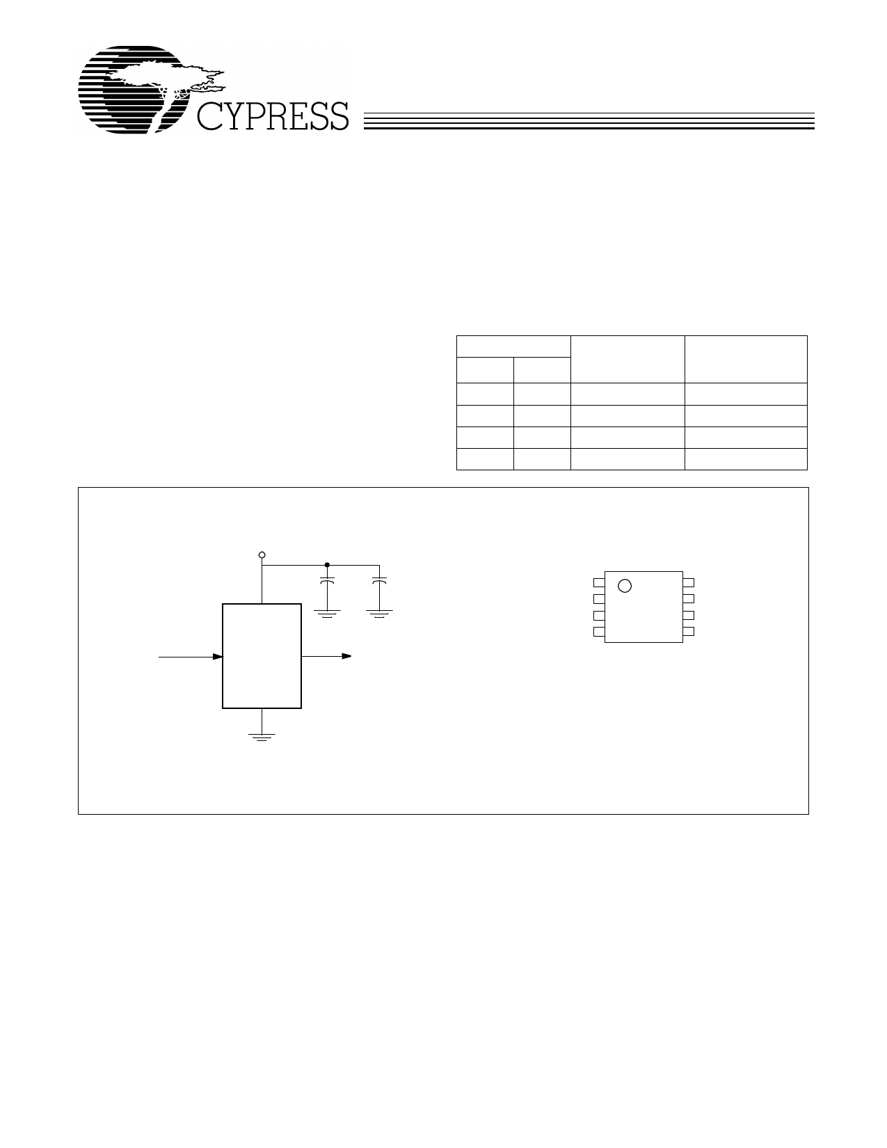
Simplified Block Diagram
3.3V or 5V
Oscillator or Reference
Input
W166
Spread Spectrum
Output
(EMI suppressed)
Pin Configuration
CLKIN
NC
GND
FS1
1
2
3
4
8 SSON#
7 CLKOUT
6 FS0
5 VDD
Cypress Semiconductor Corporation • 3901 North First Street • San Jose • CA 95134 • 408-943-2600
December 20, 1999, rev. **
1 page 
W166
DC Electrical Characteristics: 0°C < TA < 70°C, VDD = 5V ±10%
Parameter
Description
Test Condition
Min
Typ
Max
Unit
IDD Supply Current
tON Power Up Time
First locked clock cycle after
Power Good
21 40 mA
5 ms
VIL
VIH
VOL
VOH
IIL
IIH
IOL
IOH
CI
CI
RP
ZOUT
Input Low Voltage
Input High Voltage
Output Low Voltage
Output High Voltage
Input Low Current
Input High Current
Output Low Current
Output High Current
Input Capacitance
Input Capacitance
Input Pull-Up Resistor
Clock Output Impedance
Note 1
Note 1
@ 0.4V, VDD = 5V
@ 2.4V, VDD = 5V
All pins except CLKIN
CLKIN pin only
0.8 V
3.5 V
0.4 V
2.4 V
–20 µA
20 µA
24 mA
24 mA
7 pF
5 pF
500 kΩ
25 Ω
AC Electrical Characteristics: TA = 0°C to +70°C, VDD = 3.3V ±5% or 5V±10%
Symbol
Parameter
Test Condition
Min
fIN
fOUT
tR
tF
tOD
tID
tJCYC
Input Frequency
Output Frequency
Output Rise Time
Output Fall Time
Output Duty Cycle
Input Duty Cycle
Jitter, Cycle-to-Cycle
Harmonic Reduction
Input Clock
Spread Off
15-pF load, 0.8V–2.4V
15-pF load, 2.4V–0.8V
15-pF load, test at VDD/2
fout = 50 MHz, third harmonic
measured, reference board,
15-pF load
50
50
40
40
8
Typ
2
2
250
Max
65
65
5
5
60
60
300
Unit
MHz
MHz
ns
ns
%
%
ps
dB
5
5 Page | ||
| Páginas | Total 7 Páginas | |
| PDF Descargar | [ Datasheet W166.PDF ] | |
Hoja de datos destacado
| Número de pieza | Descripción | Fabricantes |
| W160A | 160 Lead Cerquad | National Semiconductor |
| W161 | 133-MHz Spread Spectrum FTG for Pentium II Platforms | Cypress Semiconductor |
| W162 | Spread Aware/ Zero Delay Buffer | Cypress Semiconductor |
| W163 | Spread Aware/ Zero Delay Buffer | Cypress Semiconductor |
| Número de pieza | Descripción | Fabricantes |
| SLA6805M | High Voltage 3 phase Motor Driver IC. |
Sanken |
| SDC1742 | 12- and 14-Bit Hybrid Synchro / Resolver-to-Digital Converters. |
Analog Devices |
|
DataSheet.es es una pagina web que funciona como un repositorio de manuales o hoja de datos de muchos de los productos más populares, |
| DataSheet.es | 2020 | Privacy Policy | Contacto | Buscar |