|
|
PDF UPD4722GS-GJG Data sheet ( Hoja de datos )
| Número de pieza | UPD4722GS-GJG | |
| Descripción | RS-232 LINE DRIVER/RECEIVER AT 3.3 V/5 V | |
| Fabricantes | NEC | |
| Logotipo |  |
|
Hay una vista previa y un enlace de descarga de UPD4722GS-GJG (archivo pdf) en la parte inferior de esta página. Total 16 Páginas | ||
|
No Preview Available !
DATA SHEET
MOS INTEGRATED CIRCUIT
µPD4722
RS-232 LINE DRIVER/RECEIVER AT 3.3 V/5 V
The µPD4722 is a high-breakdown voltage silicon gate CMOS line driver/receiver based on the EIA/TIA-232-E
standard. The internal DC/DC converter can switch between multiple voltages, allowing it to operate with a single +3.3
V or +5 V power supply. It also provides standby function.
This IC incorporates 4 driver circuits and 4 receiver circuits. An RS-232 interface circuit can be easily configured
by connecting 5 capacitors externally.
FEATURES
• Conforms to EIA/TIA-232-E (former name, RS-232C) standards
• Selectable +3.3 V/+5 V single power supply (selected by VCHA pin)
• By setting the standby pin to a low level (standby mode), circuit current can be reduced. At such times, the driver
output is in a high-impedance state.
• Even in the standby mode, 2 receiver circuits can operate as inverters without hysteresis width.
The other 2 circuits are fixed at a high level.
ORDERING INFORMATION
Part number
µPD4722GS-GJG
Package
30-pin plastic SSOP (300 mil)
Document No. S12199EJ3V0DS00 (3rd edition)
(Previous No. IC-3280)
Date Published January 1997 N
Printed in Japan
© 1993
1 page 
µPD4722
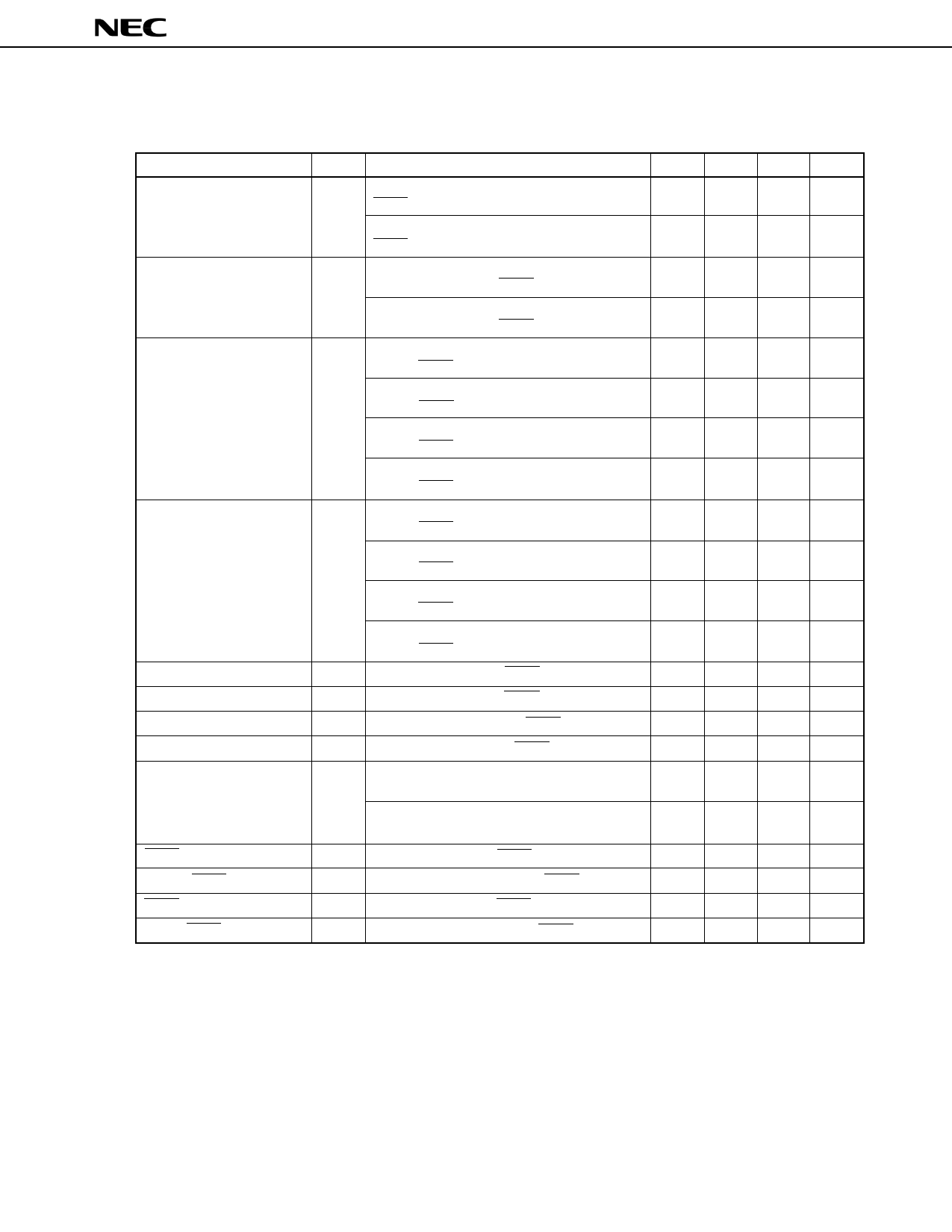
ELECTRICAL SPECIFICATIONS (TOTAL)
(UNLESS OTHERWISE SPECIFIED, TA = –40 to +85 °C, C1 to C5 = 1 µF)
Parameter
Symbol
Conditions
Circuit Current
VCC = +3.3 V, No load, RIN pin OPEN,
STBY = H
ICC1
VCC = +5.0 V, No load, RIN pin OPEN,
STBY = H
Circuit Current
VCC = +3.3 V, RL = 3 kΩ (DOUT), DIN = GND,
RIN, ROUT pin OPEN, STBY = H
ICC2
VCC = +5.0 V,RL = 3 kΩ (DOUT), DIN = GND,
RIN, ROUT pin OPEN, STBY = H
VCC = +3.3 V, No load, DIN and RIN pins are
OPEN, STBY = L, EN = L, TA = 25 °C
VCC = +3.3 V, No load, DIN and RIN pins are
Circuit Current at Standby ICC3 OPEN, STBY = L, EN = L
(Standby Mode 1)
VCC = +5.0 V, No load, DIN and RIN pins are
OPEN, STBY = L, EN = L, TA = 25 °C
VCC = +5.0 V, No load, DIN and RIN pins are
OPEN, STBY = L, EN = L
VCC = +3.3 V, No load, DIN and RIN pins are
OPEN, STBY = L, EN = H, TA = 25 °C
VCC = +3.3 V, No load, DIN and RIN pins are
Circuit Current at Standby ICC4 OPEN, STBY = L, EN = H
(Standby Mode 2)
VCC = +5.0 V, No load, DIN and RIN pins are
OPEN, STBY = L, EN = H, TA = 25 °C
VCC = +5.0 V, No load, DIN and RIN pins are
OPEN, STBY = L, EN = H
High-Level Input Voltage
VIH VCC = +3.0 to +5.5 V, STBY, VCHA, EN pin
Low-Level Input Voltage
VIL VCC = +3.0 to +5.5 V, STBY, VCHA, EN pin
High-Level Input Current
IIH VCC = +5.5 V, VI = 5.5 V, STBY, VCHA, EN pin
Low-Level Input Current
IIL VCC = +5.5 V, VI = 0 V, STBY, VCHA, EN pin
Input Capacitance
Driver input and receiver input
VCC = +3.3 V, for GND, f = 1 MHz
CIN
Driver input and receiver input
VCC = +5.0 V, for GND, f = 1 MHz
STBY — VCHA Time
VCHA — STBY Time
tSCH VCC = +3.0 to 5.5 V, STBY ↓ → VCHA, Note 8
tCHS VCC = +3.0 to 5.5 V, VCHA → STBY ↑, Note 8
STBY — VCC Time
tSC VCC = +3.0 to 5.5 V, STBY ↓ → VCC, Note 8
VCC — STBY Time
tCS VCC = +3.0 to 5.5 V, VCC → STBY ↑, Note 8
MIN.
2.4
1
1
1
1
TYP. MAX.
16
12
47
38
13
5
25
10
13
5
25
10
0.6
1
–1
10
10
Unit
mA
mA
mA
mA
µA
µA
µA
µA
µA
µA
µA
µA
V
V
µA
µA
pF
pF
µs
µs
µs
µs
* The TYP. values are for reference at TA = 25 °C.
5
5 Page 
µPD4722
Note 16. Measuring point
VCC
STBY
0V
VOH
ROUT
VOL
0.6 V
tDAH
2.0 V
2.4 V
tDHA
0.8 V
Receiver outputs are indefinite during transition time (tDHA).
Note 17. Measuring point
3.3 V
VCC
3.0 V
0V
VOH
tPRA
ROUT
VOL
0.8 V
Receiver outputs are indefinite during reset release time (tPRA).
Note 18. Measuring point
5V
VCC
4.5 V
0V
VOH
tPRA
ROUT
VOL
0.8 V
Receiver outputs are indefinite during reset release time (tPRA).
REFERENCE MATERIAL
• IC PACKAGE MANUAL (C10943X)
• NEC SEMICONDUCTOR DEVICE RELIABILITY/QUALITY (IEI-1212)
11
11 Page | ||
| Páginas | Total 16 Páginas | |
| PDF Descargar | [ Datasheet UPD4722GS-GJG.PDF ] | |
Hoja de datos destacado
| Número de pieza | Descripción | Fabricantes |
| UPD4722GS-GJG | RS-232 LINE DRIVER/RECEIVER AT 3.3 V/5 V | NEC |
| Número de pieza | Descripción | Fabricantes |
| SLA6805M | High Voltage 3 phase Motor Driver IC. |
Sanken |
| SDC1742 | 12- and 14-Bit Hybrid Synchro / Resolver-to-Digital Converters. |
Analog Devices |
|
DataSheet.es es una pagina web que funciona como un repositorio de manuales o hoja de datos de muchos de los productos más populares, |
| DataSheet.es | 2020 | Privacy Policy | Contacto | Buscar |
