|
|
PDF UPD3734ACY Data sheet ( Hoja de datos )
| Número de pieza | UPD3734ACY | |
| Descripción | 2660 PIXELS CCD LINEAR IMAGE SENSOR | |
| Fabricantes | NEC | |
| Logotipo |  |
|
Hay una vista previa y un enlace de descarga de UPD3734ACY (archivo pdf) en la parte inferior de esta página. Total 20 Páginas | ||
|
No Preview Available !
DATA SHEET
MOS INTEGRATED CIRCUIT
µPD3734A
2660 PIXELS CCD LINEAR IMAGE SENSOR
The µPD3734A is a high sensitivity CCD (Charge Coupled Device) linear image sensor which changes optical
images to electrical signal.
The µPD3734A has 2660 pixels and an output amplifier which has high gain and wide output range, but low noise.
Built-in sample and hold circuit converts and outputs independent signal from CCD register in every pixel to
continuous video signal. So it is easy to interface to A/D converter or Bi-level converter.
FEATURES
• Valid photocell
: 2660 pixels
• Photocell’s pitch
: 11 µm
• High sensitivity
: 70 V/lx·s TYP.
• Peak response wavelength : 550 nm (green)
• Resolution
: 12 dot/mm A4 (210 × 297 mm) size (shorter side)
300 dpi US letter (8.5” × 11”) size (shorter side)
• Power supply
: +12 V
• Drive clock level
: CMOS output under 5 V operation
• High speed scan
: 0.54 ms/line (S/H in used)
• Built-in circuit
: Sample and hold circuit
Reset feed-through level clamp circuit
Clamp pulse generation circuit
Voltage amplifier
• Low noise
: A quarter of the µPD3734
• Low image lag
: 1 % MAX.
• Pin assign
: Compatible with the µPD3734
ORDERING INFORMATION
Part Number
µPD3734ACY
Package
CCD linear image sensor 22-pin plastic DIP (400 mil)
The information in this document is subject to change without notice.
Document No. S11454EJ1V0DS00 (1st edition)
Date Published May 1996 P
Printed in Japan
© 1996
1 page 
µPD3734A
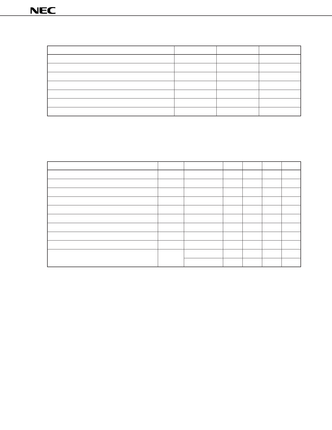
ABSOLUTE MAXIMUM RATINGS (TA = +25 ˚C)
Parameter
Output drain voltage
Shift register clock voltage
Reset gate clock voltage
Transfer gate clock voltage
Sample and hold clock voltage
Operating ambient temperature
Storage temperature
Symbol
VOD
Vφ1, Vφ2
VφRB
VφTG
VφSHB
TA
Tstg
Ratings
–0.3 to +15
–0.3 to +15
–0.3 to +15
–0.3 to +15
–0.3 to +15
–25 to +60
–40 to +70
Unit
V
V
V
V
V
˚C
˚C
Caution Exposure to ABSOLUTE MAXIMUM RATING for extended periods may affect device reliability;
exceeding the ratings could cause permanent damage. The parameters apply independently.
RECOMMENDED OPERATING CONDITIONS (TA = –25 to +60 ˚C)
Parameter
Output drain voltage
Shift register clock high level
Shift register clock low level
Reset gate clock high level
Reset gate clock low level
Transfer gate clock high level
Transfer gate clock low level
Sample and hold clock high level
Sample and hold clock low level
Data rate
Symbol
VOD
Vφ1H, Vφ2H
Vφ1L, Vφ2L
VφRBH
VφRBL
VφTGH
VφTGL
VφSHBH
VφSHBL
fφRB
Conditions
S/H in used
S/H not in used
MIN.
11.4
4.5
–0.3
4.5
–0.3
4.5
–0.3
4.5
–0.3
0.2
0.2
TYP.
12.0
5.0
0
5.0
0
5.0
0
5.0
0
1
1
MAX.
12.6
5.5
+0.5
5.5
+0.5
5.5
+0.5
5.5
+0.5
5
4
Unit
V
V
V
V
V
V
V
V
V
MHz
MHz
5
5 Page 
µPD3734A
6. Output impedance: Zo
Output pin impedance viewed from outside.
7. Response: R
Output voltage divided by exposure (lx·s).
Note that the response varies with a light source.
8. Image Lag: IL
The rate between the last output voltage and the next one after read out the data of a line.
φ TG
Light
ON
OFF
VOUT
IL (%) = V1 × 100
VOUT
VOUT
V1
9. Register Imbalance: RI
The rate of the difference between the average of the output voltage of Odd and Even pixels, against the
average output voltage of all the valid pixels.
2
n
RI (%) =
n
2
∑ (V2j−1 − V2j )
j=1
1
n
∑
Vj
n j=1
× 100
n : Number of valid pixels
Vj : Output voltage of each pixel
10. Bit Noise: BN
Output signal distribution of a photocell by scan.
11
11 Page | ||
| Páginas | Total 20 Páginas | |
| PDF Descargar | [ Datasheet UPD3734ACY.PDF ] | |
Hoja de datos destacado
| Número de pieza | Descripción | Fabricantes |
| UPD3734ACY | 2660 PIXELS CCD LINEAR IMAGE SENSOR | NEC |
| Número de pieza | Descripción | Fabricantes |
| SLA6805M | High Voltage 3 phase Motor Driver IC. |
Sanken |
| SDC1742 | 12- and 14-Bit Hybrid Synchro / Resolver-to-Digital Converters. |
Analog Devices |
|
DataSheet.es es una pagina web que funciona como un repositorio de manuales o hoja de datos de muchos de los productos más populares, |
| DataSheet.es | 2020 | Privacy Policy | Contacto | Buscar |
