|
|
|
PDF UPA1763 Data sheet ( Hoja de datos )
| Número de pieza | UPA1763 | |
| Descripción | SWITCHING DUAL N-CHANNEL POWER MOS FET INDUSTRIAL USE | |
| Fabricantes | NEC | |
| Logotipo | ||
Hay una vista previa y un enlace de descarga de UPA1763 (archivo pdf) en la parte inferior de esta página. Total 8 Páginas | ||
|
No Preview Available !
DATA SHEET
MOS FIELD EFFECT TRANSISTOR
µPA1763
SWITCHING
DUAL N-CHANNEL POWER MOS FET
INDUSTRIAL USE
DESCRIPTION
The µPA1763 is N-Channel MOS Field Effect Transistor
designed for DC/DC Converters.
FEATURES
• Dual chip type
• Low on-resistance
5 RDS(on)1 = 47.0 mΩ MAX. (VGS = 10 V, ID = 2.3 A)
5 RDS(on)2 = 57.0 mΩ MAX. (VGS = 4.5 V, ID = 2.3 A)
5 RDS(on)3 = 66.0 mΩ MAX. (VGS = 4.0 V, ID = 2.3 A)
• Low input capacitance
5 Ciss = 870 pF TYP.
• Built-in G-S protection diode
• Small and surface mount package (Power SOP8)
ORDERING INFORMATION
PART NUMBER
µPA1763G
PACKAGE
Power SOP8
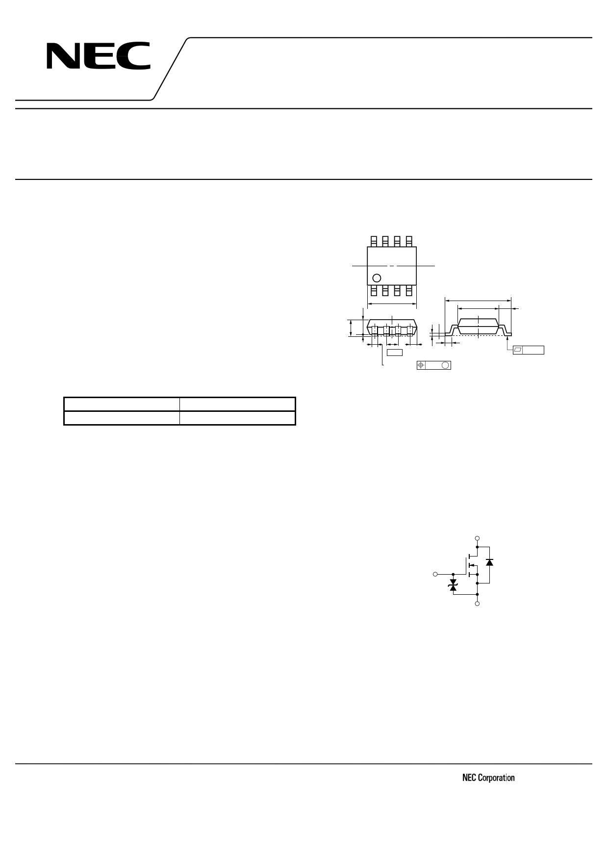
PACKAGE DRAWING (Unit : mm)
85
14
5.37 MAX.
1 : Source 1
2 : Gate 1
7, 8 : Drain 1
3 : Source 2
4 : Gate 2
5, 6 : Drain 2
6.0 ±0.3
4.4
0.8
1.27 0.78 MAX.
0.40
+0.10
–0.05
0.12 M
0.5 ±0.2
0.10
ABSOLUTE MAXIMUM RATINGS (TA = 25 °C, All terminals are connected.)
Drain to Source Voltage
VDSS 60 V
Gate to Source Voltage
Drain Current (DC)
Drain Current (pulse) Note1
Total Power Dissipation (1 unit) Note2
Total Power Dissipation (2 unit) Note2
5 Single Avalanche Current Note3
5 Single Avalanche Energy Note3
VGSS
ID(DC)
ID(pulse)
PT
PT
IAS
EAS
±20
±4.5
±18
1.7
2.0
4.5
60
V
A
A
W
W
A
mJ
EQUIVALENT CIRCUIT
(1/2 Circuit)
Drain
Gate
Body
Diode
Channel Temperature
Storage Temperature
Tch 150 °C
Tstg –55 to + 150 °C
Gate
Protection
Diode
Source
Notes 1. PW ≤ 10 µs, Duty cycle ≤ 1 %
2. TA = 25 °C, Mounted on ceramic substrate of 1200 mm2 x 2.2 mm
5 3. Starting Tch = 25 °C, RG = 25 Ω, VGS = 20 V → 0 V
Remark The diode connected between the gate and source of the transistor serves as a protector against ESD.
When this device actually used, an additional protection circuit is externally required if a voltage
Exceeding the rated voltage may be applied to this device.
The information in this document is subject to change without notice. Before using this document, please
confirm that this is the latest version.
Not all devices/types available in every country. Please check with local NEC representative for
availability and additional information.
Document No. G14056EJ1V0DS00 (1st edition)
Date Published January 2000 NS CP(K)
Printed in Japan
The mark 5 shows major revised points.
©
1999, 2000
1 page 
µPA1763
DERATING FACTOR OF FORWARD BIAS
SAFE OPERATING AREA
100
80
60
40
20
0 20 40 60 80 100 120 140 160
TA - Ambient Temperature - ˚C
TOTAL POWER DISSIPATION vs.
AMBIENT TEMPERATURE
2.8
Mounted on ceramic
substrate of
2.4 1200 mm2 × 2.2 mm
2 unit
2.0
1 unit
1.6
1.2
0.8
0.4
0 20 40 60 80 100 120 140 160
TA - Ambient Temperature - ˚C
FORWARD BIAS SAFE OPERATING AREA
100
Mounted on ceramic
substrate of
1200mm2 × 2.2 mm, 1 unit
10
1
RD(VS(GonS)
=Li1m0itVe)d
ID(DC)
TA = 25 ˚C
Single Pulse
ID(pulse)
PW
PW =100
Power
PW =1
DissiPpWati=o1n0L0im=m1iste0dms
ms
µs
0.1
0.1 1 10 100
VDS - Drain to Source Voltage - V
1000
100
TRANSIENT THERMAL RESISTANCE vs. PULSE WIDTH
Rth(ch-A) = 73.5˚C/W
10
1
0.1
0.01
100µ
1m
10 m 100 m
Mounted on ceramic
substrate of 1200mm2 × 2.2 mm
Single Pulse, 1 unit
1 10 100 1000
PW - Pulse Width - s
Data Sheet G14056EJ1V0DS00
5
5 Page | ||
| Páginas | Total 8 Páginas | |
| PDF Descargar | [ Datasheet UPA1763.PDF ] | |
Hoja de datos destacado
| Número de pieza | Descripción | Fabricantes |
| UPA1760 | SWITCHING N-CHANNEL POWER MOS FET INDUSTRIAL USE | NEC |
| UPA1763 | SWITCHING DUAL N-CHANNEL POWER MOS FET INDUSTRIAL USE | NEC |
| UPA1764 | SWITCHING DUAL N-CHANNEL POWER MOS FET INDUSTRIAL USE | NEC |
| Número de pieza | Descripción | Fabricantes |
| SLA6805M | High Voltage 3 phase Motor Driver IC. |
Sanken |
| SDC1742 | 12- and 14-Bit Hybrid Synchro / Resolver-to-Digital Converters. |
Analog Devices |
|
DataSheet.es es una pagina web que funciona como un repositorio de manuales o hoja de datos de muchos de los productos más populares, |
| DataSheet.es | 2020 | Privacy Policy | Contacto | Buscar |