|
|
PDF PCA9512D Data sheet ( Hoja de datos )
| Número de pieza | PCA9512D | |
| Descripción | Level shifting hot swappable I2C and SMBus buffer | |
| Fabricantes | NXP Semiconductors | |
| Logotipo | ||
Hay una vista previa y un enlace de descarga de PCA9512D (archivo pdf) en la parte inferior de esta página. Total 16 Páginas | ||
|
No Preview Available !
INTEGRATED CIRCUITS
PCA9512
Level shifting hot swappable
I2C and SMBus buffer
Product data sheet
2004 Oct 05
Philips
Semiconductors
1 page 
Philips Semiconductors
Level shifting hot swappable I2C and SMBus buffer
Product data sheet
PCA9512
Maximum number of devices in series
Each buffer adds about 0.065 V dynamic level offset at 25 °C with
the offset larger at higher temperatures. Maximum offset (VOS) is
0.150 V. The LOW level at the signal origination end (master) is
dependent upon the load and the only specification point is the
I2C-bus specification of 3 mA will produce VOL < 0.4 V, although if
lightly loaded the VOL may be ∼0.1 V. Assuming VOL = 0.1 V and
VOS = 0.1 V, the level after four buffers would be 0.5 V, which is only
about 0.1 V below the threshold of the rising edge accelerator (about
0.6 V). With great care a system with four buffers may work, but as
the VOL moves up from 0.1 V, noise or bounces on the line will result
in firing the rising edge accelerator thus introducing false clock
edges. Generally it is recommended to limit the number of buffers in
series to two.
The PCA9510 (rise time accelerator is permanently disabled) and
the PCA9512 (rise time accelerator can be turned off) are a little
different with the rise time accelerator turned off because the rise
time accelerator will not pull the node up, but the same logic that
turns on the accelerator turns the pull-down off. If the VIL is above
∼0.6 V and a rising edge is detected, the pull-down will turn off and
will not turn back on until a falling edge is detected; so if the noise is
small enough it may be possible to use more than two PCA9510 or
PCA9512 parts in series but is not recommended.
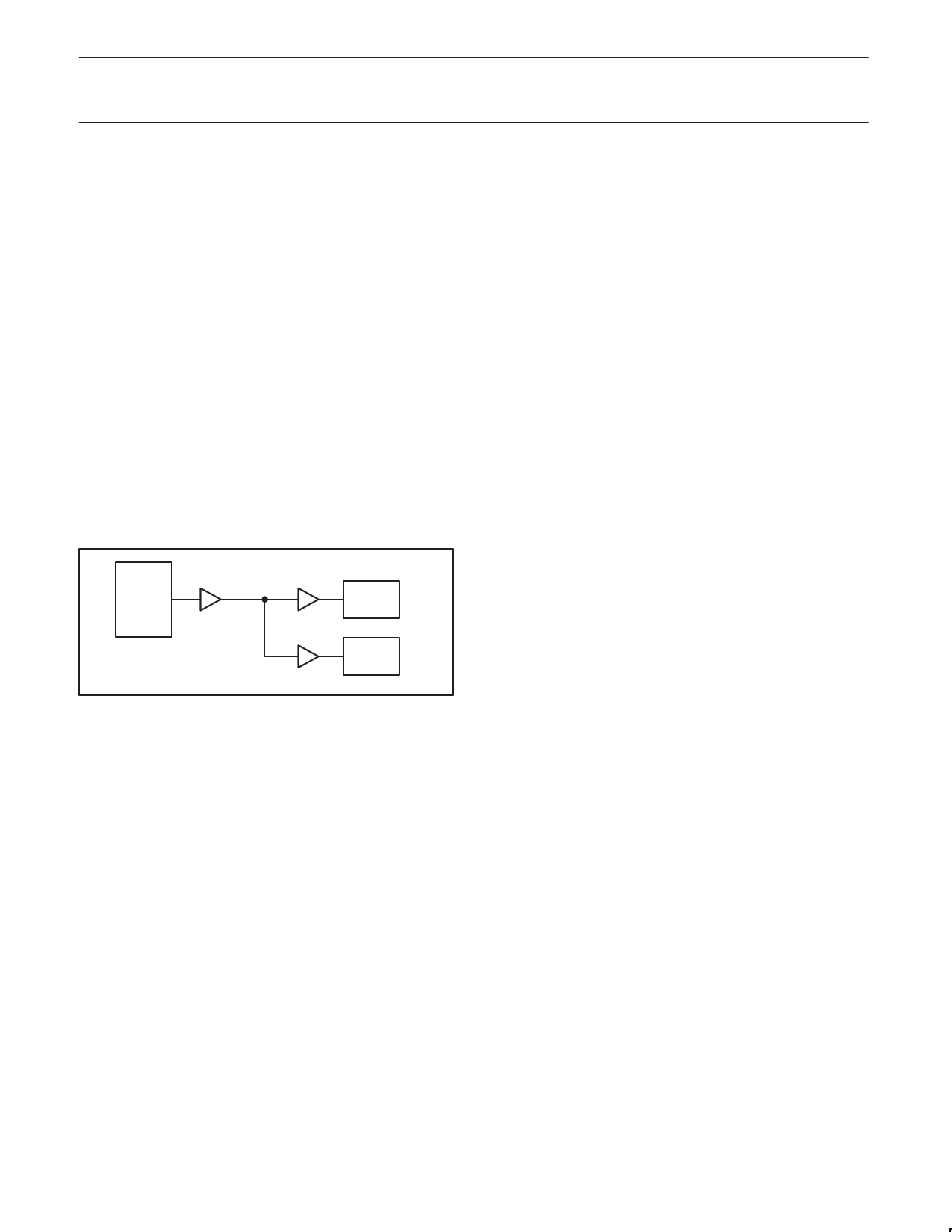
MASTER
buffer A
common
node
buffer B
SLAVE B
buffer C
SLAVE C
Figure 4.
SW02353
Consider a system with three buffers connected to a common node
and communication between the Master and Slave B that are
connected at either end of Buffer A and Buffer B in series as shown
in Figure 4. Consider if the VOL at the input of Buffer A is 0.3 V and
the VOL of Slave B (when acknowledging) is 0.4 V with the direction
changing from Master to Slave B and then from Slave B to Master.
Before the direction change you would observe VIL at the input of
Buffer A of 0.3 V and its output, the common node, is ∼0.4 V. The
output of Buffer B and Buffer C would be ∼0.5 V, but Slave B is
driving 0.4 V, so the voltage at Slave B is 0.4 V. The output of
Buffer C is ∼0.5 V. When the Master pull-down turns off, the input of
Buffer A rises and so does its output, the common node, because it
is the only part driving the node. The common node will rise to 0.5 V
before Buffer B’s output turns on, if the pull-up is strong the node will
bounce. If the bounce goes above the threshold for the rising edge
accelerator ∼0.6 V the accelerators on both Buffer A and Buffer C
will fire contending with the output of Buffer B. The node on the input
of Buffer A will go HIGH as will the input node of Buffer C. After the
common node voltage is stable for a while the rising edge
accelerators will turn off and the common node will return to ∼0.5 V
because the Buffer B is still on. The voltage at both the Master and
Slave C nodes would then fall to ∼0.6 V until Slave B turned off. This
would not cause a failure on the data line as long as the return to
0.5 V on the common node (∼0.6 V at the Master and Slave C)
occurred before the data setup time. If this were the SCL line, the
parts on Buffer A and Buffer C would see a false clock rather than a
stretched clock, which would cause a system error.
Propagation Delays
The delay for a rising edge is determined by the combined pull-up
current from the bus resistors and the PCA9512 and the effective
capacitance on the lines. If the pull-up currents are the same, any
difference in capacitance between the two sides. The tPLH may be
negative if the output capacitance is less than the input capacitance
and would be positive if the output capacitance is larger than the
input capacitance, when the currents are the same.
The tPHL can never be negative because the output does not start to
fall until the input is below 0.7VCC (or 0.7VCC2 for SDAOUT and
SCLOUT) and the output pull down turn on has a nonzero delay,
and the output has a limited maximum slew rate and even it the
input slew rate is slow enough that the output catches up it will still
lag the falling voltage of the input by the offset voltage, The
maximum tPHL occurs when the input is driven LOW with zero delay
and the output is still limited by its turn on delay and the falling edge
slew rate, The output falling edge slew rate (which is a function of
temperature, VCC or VCC2, and process) as well as load current and
load capacitance.
Rise Time Accelerators
During positive bus transitions a 2 mA current source is switched on
to quickly slew the SDA and SCL lines HIGH once the input level of
0.6 V is exceeded. The rising edge rate should be at least 1.25 V/µs
to guarantee turn on of the accelerators.
ACC Boost Current Enable
Users having lightly loaded systems may wish to disable the
rise-time accelerators. Driving this pin to ground turns off the
rise-time accelerators on all four SDA and SCL pins. Driving this pin
to the VCC2 voltage enables normal operation of the rise-time
accelerators.
2004 Oct 05
5
5 Page 
Philips Semiconductors
Level shifting hot swappable I2C and SMBus buffer
Product data sheet
PCA9512
3. The connection circuitry always regulates its output to a higher voltage than its input. The magnitude of this offset voltage as a function of
the pull-up resistor and VCC voltage is shown in the Typical Performance Characteristics section.
4. Guaranteed by design, not production tested.
5. CB = total capacitance of one bus line in pF.
6. Enable time is from power-up of VCC and VCC2 ≥ 2.7 V to when idle or stop time begins.
7. Idle time is from when SDAx and SCLx are HIGH after enable time has been met.
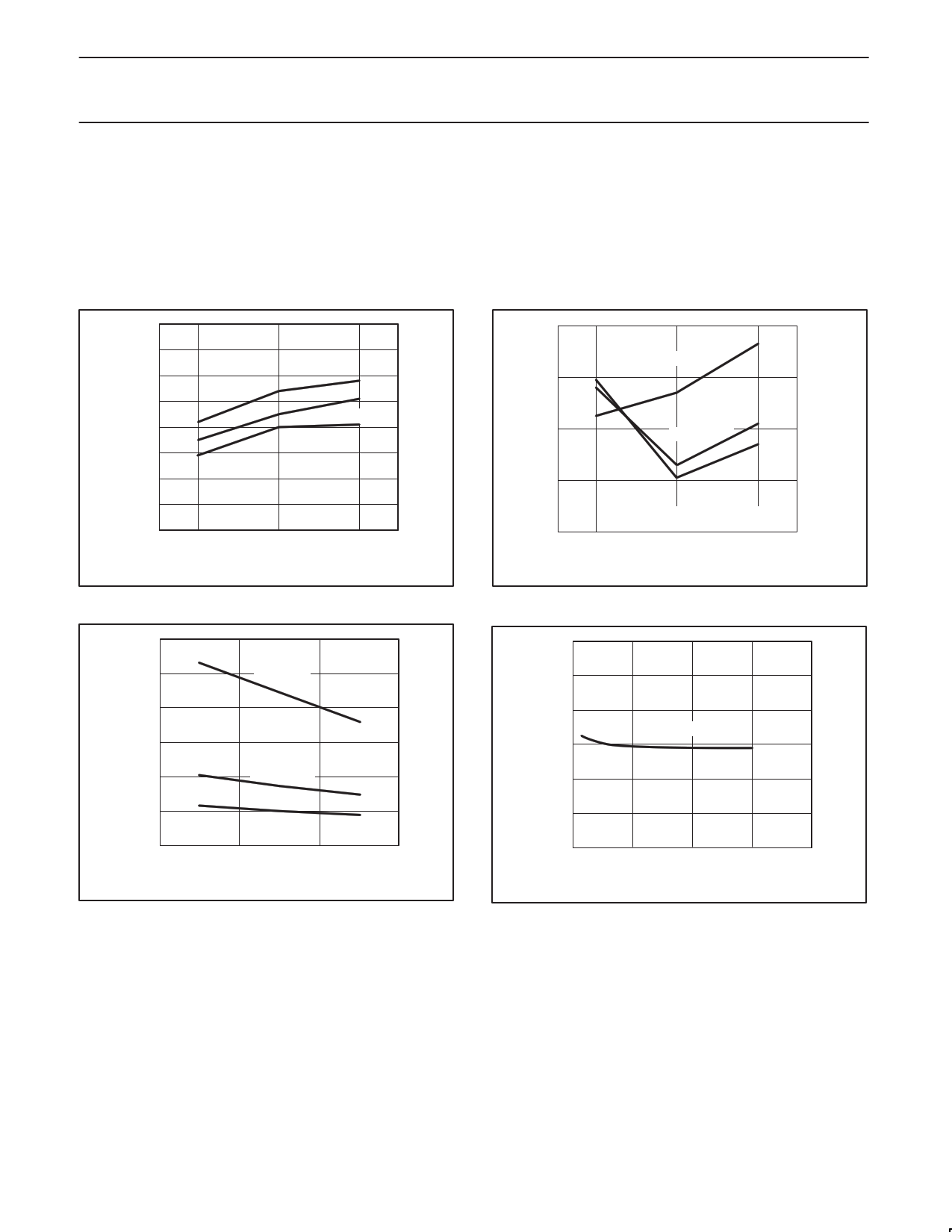
TYPICAL PERFORMANCE CHARACTERISTICS
1.5
1.4
1.3
VCC = 5.5 V
1.2
VCC = 3.3 V
1.1
VCC = 2.7 V
1.0
0.9
0.8
0.7
–40 +25 +85
TEMPERATURE (°C)
SW02343
Figure 10. ICC versus Temperature (Note 1)
12
10 VCC = 5 V
8
6
4 VCC = 3.3 V
2
VCC = 2.7 V
0
–40 +25 +85
TEMPERATURE (°C)
SW02346
Figure 11. IPULLUPAC versus Temperature
NOTE:
1. ICC2 (Pin 1) typical current averages 0.1 mA less than ICC on Pin 8.
460
VCC = 2.7 V
440
420 VCC = 5.5 V
VCC = 3.3 V
400
CIN = COUT = 100 pF
RPULLUPIN = RPULLUPOUT = 10 kΩ
380
–40 +25 +85
TEMPERATURE (°C)
SW02344
Figure 12. Input–output tPHL versus Temperature
100
90
80
VCC = 3.3 V OR 5.5 V
70
60
50
40
0
10,000
20,000
30,000
40,000
RPULLUP (Ω)
SW02154
Figure 13. Connection circuitry VOUT – VIN
2004 Oct 05
11
11 Page | ||
| Páginas | Total 16 Páginas | |
| PDF Descargar | [ Datasheet PCA9512D.PDF ] | |
Hoja de datos destacado
| Número de pieza | Descripción | Fabricantes |
| PCA9512 | Level shifting hot swappable I2C and SMBus buffer | NXP Semiconductors |
| PCA9512A | Level shifting hot swappable I2C-bus and SMBus bus buffer | NXPSemiconductors |
| PCA9512D | Level shifting hot swappable I2C and SMBus buffer | NXP Semiconductors |
| PCA9512DP | Level shifting hot swappable I2C and SMBus buffer | NXP Semiconductors |
| Número de pieza | Descripción | Fabricantes |
| SLA6805M | High Voltage 3 phase Motor Driver IC. |
Sanken |
| SDC1742 | 12- and 14-Bit Hybrid Synchro / Resolver-to-Digital Converters. |
Analog Devices |
|
DataSheet.es es una pagina web que funciona como un repositorio de manuales o hoja de datos de muchos de los productos más populares, |
| DataSheet.es | 2020 | Privacy Policy | Contacto | Buscar |
