|
|
|
PDF IDT821024 Data sheet ( Hoja de datos )
| Número de pieza | IDT821024 | |
| Descripción | QUAD NON-PROGRAMMABLE PCM CODEC | |
| Fabricantes | Integrated Device | |
| Logotipo | ||
Hay una vista previa y un enlace de descarga de IDT821024 (archivo pdf) en la parte inferior de esta página. Total 13 Páginas | ||
|
No Preview Available !
QUAD NON-PROGRAMMABLE
PCM CODEC
IDT821024
FEATURES
• 4 channelCODEC with on-chip digital filters
• Selectable A-law orµ-law companding
• Master clock frequency selection: 2.048 MHz, 4.096 MHz or
8.192 MHz
- Internal timing automatically adjusted based on MCLK and
frame sync signal
• Separate PCM and master clocks
• Single PCM port with up to 8.192 MHz data rate (128 time slots)
• Transhybridbalanceimpedancehardwareadjustableviaexternal
components
• Transmitgainshardwareadjustableviaexternalcomponents
• Low power +5.0 V CMOS technology
• +5.0 V single power supply
• Package available: 32 pin PLCC, 44 pin TQFP
DESCRIPTION
The IDT821024 is a single-chip, four channel PCM CODEC with on-
chip filters. The device provides analog-to-digital and digital-to-analog
conversions and supports both a-law and µ−law companding. The digital
filters in IDT821024 provides the necessary transmit and receive filtering
for voice telephone circuit to interface with time-division multiplexed
systems. All of the digital filters are performed in digital signal processors
operating from an internal clock, which is derived from MCLK. The fixed
filters set the transmit and receive gain and frequency response.
In the IDT821024 the PCM data is transmitted to and received from
the PCM highway in time slots determined by the individual Frame Sync
sMigHnza.lsB(oFthSRLnoanngdaFnSdXSn,hworhteFreranm=e1S-4y)nact
rates from 256 KHz to
modes are available
8.192
in the
IDT821024.
The IDT821024 can be used in digital telecommunication applications
such as PBX, Central Office Switch, Digital Telephone and Integrated Voice/
Data Access Unit.
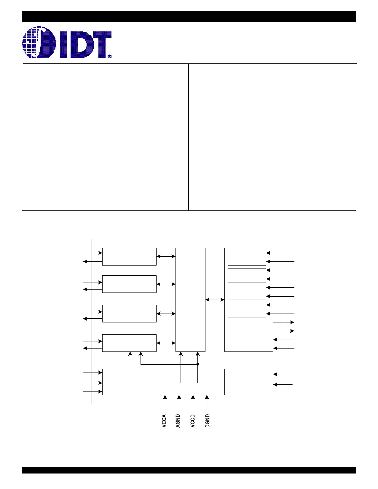
FUNCTIONAL BLOCK DIAGRAM
IIN1
VOUT1
IIN2
VOUT2
IIN3
VOUT3
IIN4
VOUT4
MCLK
IREF
CNF
Anolog Front End
CH1
Anolog Front End
CH2
Anolog Front End
CH3
Anolog Front End
CH4
Clock
&
Reference Circuits
DSP
PCM TSA 1
PCM TSA 2
PCM TSA 3
PCM TSA 4
PCM Interface
Control
FSX1
FSR1
FSX2
FSR2
FSX3
FSR3
FSX4
FSR4
DX
TSC
DR
PCLK
PDN 1~ 4
A/µ
The IDT logo is a registered trademark of Integrated Device Technology, Inc
INDUSTRIAL TEMPERATURE RANGE
©2003 Integrated Device Technology, Inc.
1
APRIL 3, 2003
DSC-6034/4
1 page 
IDT821024 QUAD NON-PROGRAMMABLE PCM CODEC
INDUSTRIAL TEMPERATURE RANGE
FUNCTIONAL DESCRIPTION
The IDT821024 contains four channel PCM CODEC with on chip digital
filters. It provides the four-wire solution for the subscriber line circuitry in
digital switches. The device converts analog voice signal to digital PCM
data, and converts digital PCM data back to analog signal. Digital filters
are used to bandlimit the voice signals during the conversion. Either A-law
or µ-law is supported by the IDT821024. The law selection is performed
by A/µ pin.
The frequency of the master clock (MCLK) can be 2.048 MHz, 4.096
MHz, or 8.192 MHz. Internal circuitry determines the master clock frequency
automatically.
The serial PCM data for four channels are time multiplexed via two pins,
DX and DR. The time slots of the four channels are determined by the
individual Frame Sync signals at rates from 256 kHz to 8.192 MHz. For
each channel, the IDT821024 provides a transmit Frame Sync signal and
a receive Frame Sync signal.
Each channel of the IDT821024 can be powered down independently
to save power consumption. The Channel Power Down Pins PDN1-4
configure channels to be active (power-on) or standby (power-down)
separately.
Signal Processing
High performance oversampling Analog-to-Digital Converters (ADC) and
Digital-to-Analog Converters (DAC) are used in the IDT821024 to provide
the required conversion accuracy. The associated decimation and interpo-
lation filtering are realized with both dedicated hardware and Digital Signal
Processor (DSP). The DSP also handles all other necessary functions such
as PCM bandpass filtering and sample rate conversion.
Transmit Signal Processing
In the transmit path, the analog input signal is received by the ADC and
converted into digital data. The digital output of the oversampling ADC is
decimated and sent to the DSP. The transmit filter is implemented in the
DSP as a digital bandpass filter. The filtered signal is further decimated
and compressed to PCM format.
Transmit PCM Interface
The transmit PCM interface clocks out 1 byte (8 bits) PCM data out of
DX pin every 125 µs. The transmit logic, synchronized by the Transmit
Frame Sync signal (FSXn), controls the data transmission. The FSXn
pulse identifies the transmit time slot of the PCM frame for Channel N.
The PCM Data is transmitted serially on DX pin with the Most Significant
Bit (MSB) first. When the PCM data is being output on DX pin, the TSC
signal will be pulled low.
Receive Signal Processing
In the receive path, the PCM code is received at the rate of 8,000 samples
per second. The PCM code is expanded and sent to the DSP for
interpolation. A receive filter is implemented in the DSP as a digital lowpass
filter. The filtered signal is then sent to an oversampling DAC. The DAC
output is post-filtered and delivered at VOUT pin by an amplifier. The
amplifier can drive resistive load higher than 2 KΩ.
Receive PCM Interface
The receive PCM interface clocks 1 byte (8 bits) PCM data into DR pin
every 125 µs. The receive logic, synchronized by the Receive Frame Sync
signal (FSRn), controls the data receiving process. The FSRn pulse
identifies the receive time slot of the PCM frame for Channel N. The PCM
Data is received serially on DR pin with the Most Significant Bit (MSB)
first.
Hardware Gain Setting In Transmit Path
The transmit gain of the IDT821024 for each channel can be set by 2
rinegsisetqoursa,tiRonRE:F and RTXn (as shown in Figure 1), according to the follow-
Gt
=
3 ×RREF
R TXn
The receive gain of IDT821024 is fixed and equal to 1.
to
SLIC
VTX RTX1
CTX1
IDT821024
A/D
VIN1 IREF
VREF
to
IREF1 RREF1
Bal
Net
IREF VREF1 CFIL
to
SLIC
RSN
RRX1
CRX1
VOUT1
VREF
D/A
Figure 1. IDT821024 Transmit Gain Setting for Channel 1
5
5 Page 
IDT821024 QUAD NON-PROGRAMMABLE PCM CODEC
INDUSTRIAL TEMPERATURE RANGE
TIMING CHARACTERISTICS
Clock
Parameter
t1
t2
t3
t4
t5
Description
PCLK Duty Cycle
PCLK Rise and Fall Time
MCLK Duty Cycle
MCLK Rise and Fall Time
PCLK Clock Period
Min Typ Max Units
Test Conditions
40 60 % PCLK=512kHz to 8.192MHz
25 ns PCLK=512kHz to 8.192MHz
40 60 % MCLK=2.048Hz,4.096MHz
or 8.192MHz
15 ns MCLK=2.048Hz,4.096MHz
or 8.192MHz
244 ns PCLK=512kHz to 8.192MHz
Transmit
Parameter
t11
t12
t13
Description
Data Output Delay Time (for Short
Frame Sync Mode)
Data Hold Time
Data Delay to High-Z
Min
5
5
50
t14 Frame sync Hold Time
50
t15 Frame sync High Setup Time
55
t16 TSC Enable Delay Time(for Short 5
Frame Sync Mode)
t17 TSC Disable Delay Time
50
t18 Data Output Delay Time(for Long 5
Frame Sync Mode)
t19 TSC Enable Delay Time(for Long 5
Frame Sync Mode)
t21 Receive Data Setup Time
25
t22 Receive Data Hold Time
5
Note: Timing parameter t13 is referenced to a high-impedance state.
Typ Max
70
70
220
t5+70
t5-50
80
220
t5+70
40
40
Units
ns
ns
ns
ns
ns
ns
ns
ns
ns
ns
ns
Test Conditions
MCLK
t4 t4
Figure 2. MCLK Timing
11
11 Page | ||
| Páginas | Total 13 Páginas | |
| PDF Descargar | [ Datasheet IDT821024.PDF ] | |
Hoja de datos destacado
| Número de pieza | Descripción | Fabricantes |
| IDT821024 | QUAD NON-PROGRAMMABLE PCM CODEC | Integrated Device |
| IDT821024J | QUAD NON-PROGRAMMABLE PCM CODEC | Integrated Device |
| IDT821024PP | QUAD NON-PROGRAMMABLE PCM CODEC | Integrated Device |
| Número de pieza | Descripción | Fabricantes |
| SLA6805M | High Voltage 3 phase Motor Driver IC. |
Sanken |
| SDC1742 | 12- and 14-Bit Hybrid Synchro / Resolver-to-Digital Converters. |
Analog Devices |
|
DataSheet.es es una pagina web que funciona como un repositorio de manuales o hoja de datos de muchos de los productos más populares, |
| DataSheet.es | 2020 | Privacy Policy | Contacto | Buscar |