|
|
|
PDF IDT7M1024 Data sheet ( Hoja de datos )
| Número de pieza | IDT7M1024 | |
| Descripción | 4K x 36 BiCMOS SYNCHRONOUS DUAL-PORT STATIC RAM MODULE | |
| Fabricantes | Integrated Device | |
| Logotipo | ||
Hay una vista previa y un enlace de descarga de IDT7M1024 (archivo pdf) en la parte inferior de esta página. Total 8 Páginas | ||
|
No Preview Available !
Integrated Device Technology, Inc.
4K x 36 BiCMOS
SYNCHRONOUS DUAL-PORT
STATIC RAM MODULE
IDT7M1024
FEATURES:
• High-density 4K x 36 Synchronous Dual-Port SRAM
module
• Architecture based on Dual-Port RAM cells
— Allows full simultaneous access from both ports
• Synchronous operation
— 4ns set-up to clock, 1ns hold on all control, data, and
address inputs
— Data input, address, and control registers
— Fast 20ns clock to data out
— Self-timed write allows fast write cycle
• Clock enable feature
• Single 5V (±10%) power supply
• Multiple GND pins and decoupling capacitors for maxi-
mum noise immunity
• Inputs/outputs directly TTL-compatible
DESCRIPTION:
The IDT7M1024 is a 4K x 36 bit high-speed synchronous
Dual-Port Static RAM module constructed on a co-fired ce-
ramic substrate using four IDT7099 (4K x 9) Dual-Port RAMs.
The IDT7M1024 module is designed to be used as a stand-
alone 36-bit Dual-Port Static RAM.
The IDT7M1024 provides a true synchronous Dual-Port
Static RAM interface. Registered inputs provide very short
set-up and hold times on address, data, and all critical control
inputs. All internal registers are clocked on the rising edge of
the clock signal. An asynchronous output enable is provided
to ease asynchronous bus interfacing.
The internal write pulse width is independent of the HIGH
and LOW periods of the clock. This allows the shortest
possible realized cycle times. Clock enable inputs are pro-
vided to stall the operation of the address and data input
registers without introducing clock skew for very fast inter-
leaved memory applications.
The data inputs are gated to control on-chip noise in bussed
applications. The user must guarantee that the R/W pins are
LOW for at least one clock cycle before any write is attempted.
A HIGH on the CE input for one clock cycle will power down the
internal circuitry to reduce static power consumption.
The IDT7M1024 module is packaged in a 142-lead ceramic
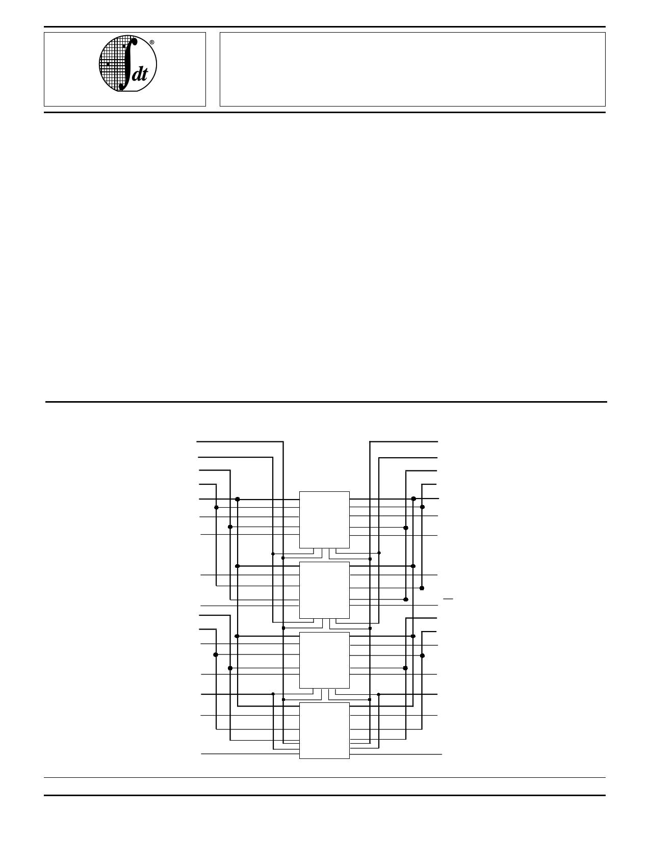
FUNCTIONAL BLOCK DIAGRAM
L_CLK
L_CLKENL
L_CEL
L_OEL
L_A0 – 11
L_I/O0 – 8
L_ R/W0
IDT7099
4K x 9
R_CLK
R_CLKENL
R_CEL
R_OEL
R_A0 – 11
R_I/O0 – 8
R_ R/W0
L_I/O9 – 17
L_ R/W1
L_CEH
L_OEH
L_I/O18 – 26
L_ R/W2
L_CLKENH
IDT7099
4K x 9
IDT7099
4K x 9
L_I/O27 – 35
IDT7099
4K x 9
L_ R/W3
The IDT logo is a registered trademark of Integrated Device Technology, Inc.
MILITARY AND COMMERCIAL TEMPERATURE RANGES
©1996 Integrated Device Technology, Inc.
7.4
R_I/O9 – 17
R_ R/W1
R_CEH
R_OEH
R_I/O18 – 26
R_ R/W2
R_CLKENH
R_I/O27 – 35
R_ R/W3
2809 drw 01
MARCH 1996
DSC-2809/6
1
1 page 
IDT7M1024
4K x 36 BiCMOS SYNCHRONOUS DUAL-PORT STATIC RAM MODULE
AC TEST CONDITIONS
Input Pulse Levels
Input Rise/Fall Times
Input Timing Reference Levels
Output Reference Levels
Output Load
GND to 3.0V
3ns
1.5V
1.5V
See Figures 1, 2 and 3
2909 tbl 10
MILITARY AND COMMERCIAL TEMPERATURE RANGES
DATA OUT
Zo = 50Ω
Figure 1. Output Load
50Ω
1.5V
2809 drw 03
DATA OUT
775Ω
5V
1250Ω
5pF*
2809 drw 04
Figure 2. Output Load (for tCLZ, tCHZ, tOLZ, and tOHZ)
*Including scope and jig.
8
7
6
∆TAA
(Typical, ns)
5
4
3
2
1
20 40 60 80 100 120 140 160 180 200
Capacitance (pF)
2809 drw 05
Figure 3. Lumped Capacitive Load, Typical Derating
AC ELECTRICAL CHARACTERISTICS OVER THE OPERATING TEMPERATURE RANGE —
(READ AND WRITE CYCLE TIMING)
(Commercial: VCC = 5V ± 10%, TA = 0°C to +70°C; Military: VCC = 5V ± 10%, TA = –55°C to +125°C)
7M1024SxxG, 7M1024SxxGB
–20 –25
–30
Symbol
Parameter
Min. Max. Min. Max. Min. Max. Unit
tCLK Clock Cycle Time
20 —
25 — 30 — ns
tCLKH Clock HIGH Time
8—
10 — 12 — ns
tCLKL Clock LOW Time
8—
10 — 12 — ns
tCQV Clock HIGH to Output Valid
— 20
— 25 — 30 ns
tRSU Registered Signal Set-up Time
5—
6 — 7 — ns
tRHD Registered Signal Hold Time
2—
2 — 2 — ns
tCOH Data Output Hold After Clock HIGH
3—
3 — 3 — ns
tCLZ Clock HIGH to Output Low-Z
2—
2 — 2 — ns
tCHZ Clock HIGH to Output High-Z
29
2 12 2 15 ns
tOE Output Enable to Output Valid
— 10
— 12 — 15 ns
tOLZ Output Enable to Output Low-Z
0—
0 — 0 — ns
tOHZ Output Disable to Output High-Z
—9
— 11 — 14 ns
tCSU Clock Enable, Disable Set-up Time
5—
6 — 7 — ns
tCHD Clock Enable, Disable Hold Time
3—
3 — 3 — ns
Port-to-Port Delay
tCWDD Write Port Clock HIGH to Read Data Delay
— 35
— 45 — 55 ns
2809 tbl 11
7.4 5
5 Page | ||
| Páginas | Total 8 Páginas | |
| PDF Descargar | [ Datasheet IDT7M1024.PDF ] | |
Hoja de datos destacado
| Número de pieza | Descripción | Fabricantes |
| IDT7M1024 | 4K x 36 BiCMOS SYNCHRONOUS DUAL-PORT STATIC RAM MODULE | Integrated Device |
| Número de pieza | Descripción | Fabricantes |
| SLA6805M | High Voltage 3 phase Motor Driver IC. |
Sanken |
| SDC1742 | 12- and 14-Bit Hybrid Synchro / Resolver-to-Digital Converters. |
Analog Devices |
|
DataSheet.es es una pagina web que funciona como un repositorio de manuales o hoja de datos de muchos de los productos más populares, |
| DataSheet.es | 2020 | Privacy Policy | Contacto | Buscar |