|
|
|
PDF IDT7M1002 Data sheet ( Hoja de datos )
| Número de pieza | IDT7M1002 | |
| Descripción | 16K x 32 CMOS DUAL-PORT STATIC RAM MODULE | |
| Fabricantes | Integrated Device | |
| Logotipo | ||
Hay una vista previa y un enlace de descarga de IDT7M1002 (archivo pdf) en la parte inferior de esta página. Total 12 Páginas | ||
|
No Preview Available !
Integrated Device Technology, Inc.
16K x 32 CMOS
DUAL-PORT STATIC RAM
MODULE
IDT7M1002
FEATURES
• High-density 512K CMOS Dual-Port RAM module
• Fast access times
—Commercial: 30, 35ns
—Military: 40, 45ns
• Fully asynchronous read/write operation from either port
• Easy to expand data bus width to 64 bits or more using
the Master/Slave function
• Separate byte read/write signals for byte control
• On-chip port arbitration logic
• INT flag for port-to-port communication
• Full on-chip hardware support of semaphore signaling
between ports
• Surface mounted fine pitch (25 mil) LCC packages allow
through-hole module to fit into 121 pin PGA footprint
• Single 5V (±10%) power supply
• Inputs/outputs directly TTL-compatible
DESCRIPTION
The IDT7M1002 is a 16K x 32 high-speed CMOS Dual-Port
Static RAM Module constructed on a co-fired ceramic sub-
strate using four 16K x 8 (IDT7006) Dual-Port Static RAMs in
surface-mounted LCC packages. The IDT7M1002 module is
designed to be used as stand-alone 512K Dual-Port RAM or
as a combination Master/Slave Dual-Port RAM for 64-bit or
more word width systems. Using the IDT Master/Slave ap-
proach in such system applications results in full-speed, error-
free operation without the need for additional discrete logic.
The module provides two independent ports with separate
control, address, and I/O pins that permit independent and
asynchronous access for reads or writes to any location in
memory. System performance is enhanced by facilitating
port-to-port communication via additional control signals SEM
and INT.
The IDT7M1002 module is packaged in a ceramic 121 pin
PGA (Pin Grid Array)1.35 inches on a side. Maximum access
times as fast as 30ns are available over the commercial
temperature range and 40ns over the military temperature
range.
All IDT military modules are constructed with semiconduc-
tor components manufactured in compliance with the latest
revision of MIL-STD-883, Class B making them ideally suited
to applications demanding the highest level of performance
and reliability.
PIN CONFIGURATION
12
34
56
7 8 9 10 11 12 13
A L_I/O(24) L_I/O(26) L_I/O(28) L_I/O(30) L_CS
B L_I/O(23) L_I/O(25) L_I/O(27) L_I/O(29) L_I/O(31)
C L_I/O(21) L_I/O(22) VCC
L_A(3) L_A(2)
D L_I/O(19) L_I/O(20)
E L_I/O(17) L_I/O(18)
F L_SEM L_I/O(16)
G L_BUSY L_INT
H L_R/W(1) L_R/W(2)
I L_I/O(15) L_I/O(14)
J L_I/O(13) L_I/O(12)
K L_I/O(11)
M/S
L_A(4)
L_A(5)
L_A(6)
GND
L_A(7)
L_A(8)
L_A(9)
GND
GND
L_A(10) L_A(11)
L L_I/O(10) L_I/O(8) L_I/O(6) L_I/O(4) L_I/O(2)
L_OE
L_A(0)
L_A(1)
L_A(12)
L_A(13)
L_R/W(3)
L_R/W(4)
GND
R_OE
R_A(0)
R_A(1)
R_CS R_I/O(30) R_I/O(28) R_I/O(26) R_I/O(24)
R_I/O(31) R_I/O(29) R_I/O(27) R_I/O(25) R_I/O(23)
R_A(2) R_A(3)
GND R_I/O(22) R_I/O(21)
R_A(4) R_I/O(20) R_I/O(19)
PGA
TOP VIEW
GND R_A(12) R_A(11)
R_A(10)
R_A(5)
R_A(6)
GND
R_A(7)
R_A(8)
R_A(9)
VCC
R_I/O(18) R_I/O(17)
R_I/O(16) R_SEM
R_INT R_BUSY
R_R/W (2) R_R/W (1)
R_I/O(14) R_I/O(15)
R_I/O(12) R_I/O(13)
GND R_I/O(11)
R_R/W (4) R_A(13) R_I/O(2) R_I/O(4) R_I/O(6) R_I/O(8) R_I/O(10)
M L_I/O(9) L_I/O(7) L_I/O(5) L_I/O(3) L_I/O(1) L_I/O(0) R_R/W (3) R_I/O(0) R_I/O(1) R_I/O(3) R_I/O(5) R_I/O(7) R_I/O(9)
2795 drw 01
The IDT logo is a registered trademark of Integrated Device Technology Inc.
MILITARY AND COMMERCIAL TEMPERATURE RANGES
©1996 Integrated Device Technology, Inc.
7.02
DECEMBER 1995
DSC-2795/5
1
1 page 
IDT7M1002
16K x 32 CMOS DUAL-PORT STATIC RAM MODULE
MILITARY AND COMMERCIAL TEMPERATURE RANGES
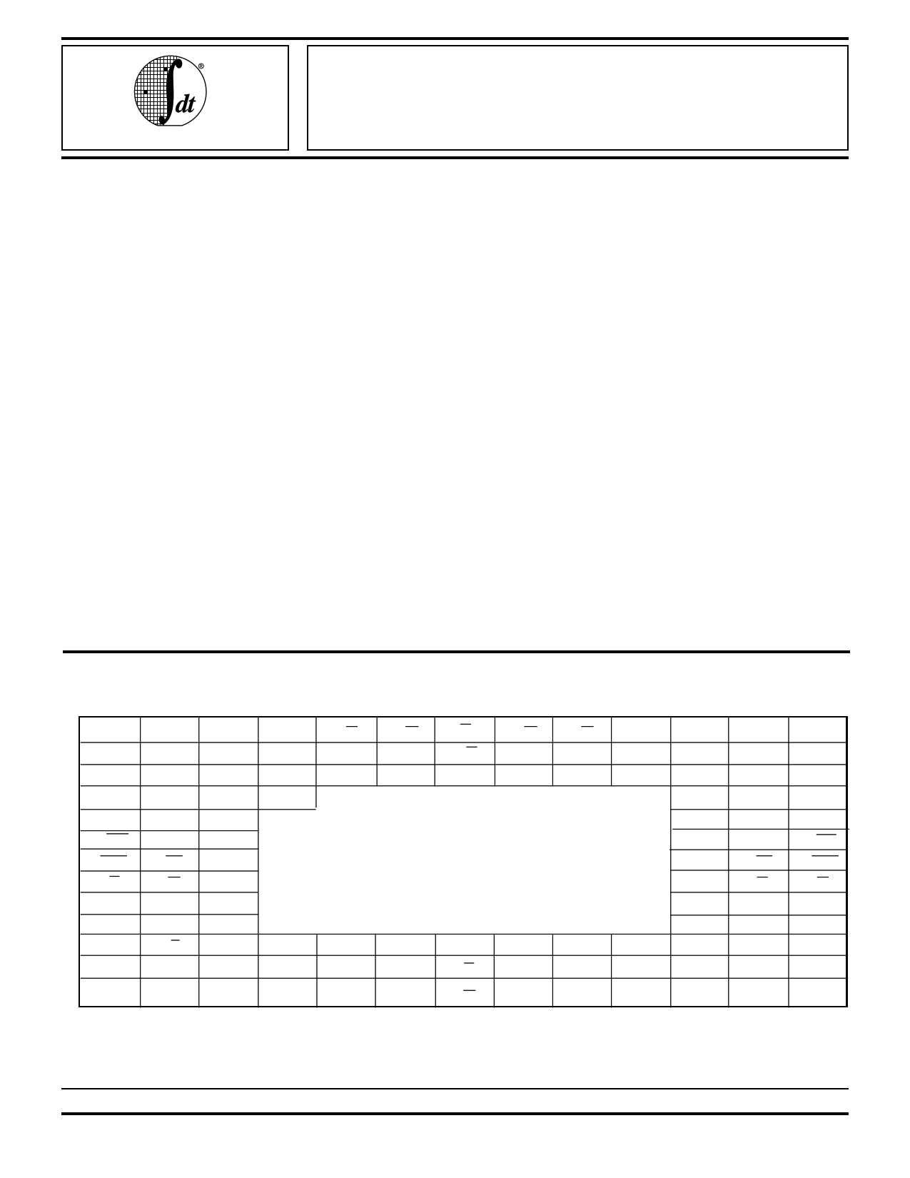
AC ELECTRICAL CHARACTERISTICS
(VCC = 5V ± 10%, TA = 55°C to +125°C or 0°C to +70°C)
Symbol Parameter
Write Cycle (continued)
tDW Data Valid to End-of-Write
tDH
tHZ(1)
tOW(1)
Data Hold Time
Output to High-Z
Output Active from End-of-Write
tSWRD
SEM Flag Write to Read Time
tSPS SEM Flag Contention Window
Busy Cycle-Master Mode(3)
tBAA
BUSY Access Time to Address
tBDA
BUSY Disable Time to Address
tBAC
BUSY Access Time to Chip Select
tBDC
tWDD(5)
BUSY Disable Time to Chip Deselect
Write Pulse to Data Delay
tDDD
tAPS(6)
Write Data Valid to Read Data Delay
Arbitration Priority Set-Up Time
tBDD
BUSY Disable to Valid Time
Busy Cycle-Slave Mode (4)
tWB(7)
Write to BUSY Input
tWH(8)
Write Hold after BUSY
tWDD(5) Write Pulse to Data Delay
Interrupt Timing
tAS Address Set-Up Time
tWR Write Recovery Time
tINS Interrupt Set Time
tINR Interrupt Reset Time
7M1002SxxG
30 –35
Min. Max. Min. Max.
22 — 25
0—0
— 15 —
0—0
10 — 10
10 — 10
—
—
15
—
—
—
— 30 —
— 25 —
— 25 —
— 25 —
— 55 —
— 40 —
5—5
— NOTE 9 —
35
30
30
25
60
45
—
NOTE 9
0—0
25 — 25
— 55 —
—
—
60
0—0
0—0
— 25 —
— 25 —
—
—
30
30
NOTES:
1. This parameter is guaranteed by design but not tested.
2. To access RAM, CS ≤ VIL and SEM ≥ VIH. To access semaphore, CS ≥ VIH and SEM ≤ VIL.
3. When the module is being used in the Master Mode (M/S ≥ VIH).
4. When the module is being used in the Slave Mode (M/S ≤ VIL).
5. Port-to-Port delay through the RAM cells from the writing port to the reading port.
6. To ensure that the earlier of the two ports wins.
7. To ensure that the write cycle is inhibited during contention.
8. To ensure that a write cycle is completed after contention.
9. tBDD is a calculated parameter and is the greater of 0, tWDD - tWP (actual), or tDDD - tWP (actual).
7M1002SxxGB
–40 –45
Min. Max. Min. Max. Unit
25 —
0—
— 17
0—
10 —
10 —
25 —
0—
— 20
0—
10 —
10 —
ns
ns
ns
ns
ns
ns
— 35
— 30
— 30
— 25
— 65
— 50
5—
— NOTE 9
— 35
— 30
— 30
— 25
— 70
— 55
5—
— NOTE 9
ns
ns
ns
ns
ns
ns
ns
ns
0—
25 —
— 65
0—
25 —
— 70
ns
ns
ns
0—
0—
— 32
— 32
0 — ns
0 — ns
— 35 ns
— 35 ns
2795 tbl 10
7.02 5
5 Page 
IDT7M1002
16K x 32 CMOS DUAL-PORT STATIC RAM MODULE
MILITARY AND COMMERCIAL TEMPERATURE RANGES
TIMING WAVEFORM OF INTERRUPT CYCLE(1)
ADDR "A"
CE "A"
tAS (3)
tWC
INTERRUPT SET ADDRESS (2)
tWR (4)
R/W 1"A"
INT "B"
ADDR "B"
CE "B"
tINS (3)
tAS (3)
tRC
INTERRUPT CLEAR ADDRESS(2)
2795 drw 16
OE "B"
tINR (3)
INT "B"
NOTES:
1. All timing is the same for left and right ports. Port “A” may be either the left or right port. Port “B” is the port opposite from “A”.
2. See Interrupt truth table.
3. Timing depends on which enable signal is asserted last.
4. Timing depends on which enable signal is de-asserted first.
2795 drw 17
TRUTH TABLE I: Non-Contention Read/Write Control(1)
Inputs
CS R/W OE SEM
HXXH
L LXH
LHLH
XXHX
NOTE:
1. The conditions for non-contention are L_A (0–13) ≠ R_A (0–13).
2. denotes a LOW to HIGH waveform transition.
TRUTH TABLE II: Semaphore Read/Write Control
Inputs(2)
CS R/W OE SEM
HHL L
H XL
LXXL
Outputs
I/O
High-Z
Data_In
Data_OUT
High-Z
Outputs
I/O
Data_OUT
Data_IN
—
Mode
Description
Deselected or Power Down
Write
Read
Outputs Disabled
2795 tbl 13
Mode
Description
Read Data in Semaphore Flag
Write Data_IN (0, 8, 16, 24)
Not Allowed
2795 tbl 14
7.02 11
11 Page | ||
| Páginas | Total 12 Páginas | |
| PDF Descargar | [ Datasheet IDT7M1002.PDF ] | |
Hoja de datos destacado
| Número de pieza | Descripción | Fabricantes |
| IDT7M1001 | 128K x 8 64K x 8 CMOS DUAL-PORT STATIC RAM MODULE | Integrated Device |
| IDT7M1002 | 16K x 32 CMOS DUAL-PORT STATIC RAM MODULE | Integrated Device |
| IDT7M1003 | 128K x 8 64K x 8 CMOS DUAL-PORT STATIC RAM MODULE | Integrated Device |
| Número de pieza | Descripción | Fabricantes |
| SLA6805M | High Voltage 3 phase Motor Driver IC. |
Sanken |
| SDC1742 | 12- and 14-Bit Hybrid Synchro / Resolver-to-Digital Converters. |
Analog Devices |
|
DataSheet.es es una pagina web que funciona como un repositorio de manuales o hoja de datos de muchos de los productos más populares, |
| DataSheet.es | 2020 | Privacy Policy | Contacto | Buscar |